正在加载图片...
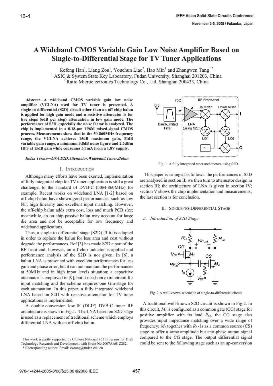
16-4 IEEE Asian Solid-State Circuits Conference November 3-5,2008/Fukuoka,Japan A Wideband CMOS Variable Gain Low Noise Amplifier Based on Single-to-Differential Stage for TV Tuner Applications Kefeng Han',Liang Zou',Youchun Liao2,Hao Min'and Zhangwen Tang'' ASIC System State Key Laboratory,Fudan University,Shanghai 201203,China 2 Ratio Microelectronics Technology Co.,Ltd,Shanghai 200433,China Abstract-A wideband CMOS variable gain low noise 75Q RF Front-end amplifier (VGLNA)used for TV tuner is presented.A Up Mixer Down Mixer single-to-differential (S2D)circuit other than an off-chip balun is applied for high gain mode and a resistive attenuator is for five steps (6dB per step)attenuation in low gain mode.The performance of S2D,especially the noise factor is analyzed.The Band-Limited LNA chip is implemented in a 0.18-um 1P6M mixed-signal CMOS Filter (using S2D) process.Measurements show that in the 50-860MHz frequency range,the VGLNA achieves 15dB maximum gain,31dB LO1 LO2 variable gain range,a minimum 3.8dB noise figure and 2.6dBm IIP3 at 15dB gain while consumes 5.7mA from a 1.8V supply. PLL Q Index Terms-LNA,S2D,Attenuator,Wideband,Tuner,Balun Fig.1 A fully integrated tuner architecture using S2D I.INTRODUCTION Although many efforts have been exerted,implementation This paper is arranged as follows:the performances of S2D of fully integrated chip for TV tuner application is still a great are analyzed in section II;we then turn to attenuator design in challenge,to the standard of DVB-C (50M-860MHz)for section Il;the architecture of LNA is given in section IV; example.Recent works on wideband LNA [1-2]based on section V shows the chip implementation and measurements; off-chip balun have shown good performances,such as low the last section is for conclusion. NF,high linearity and excellent input matching.However, the off-chip balun adds extra cost,loss and much PCB size; II.SINGLE-TO-DIFFERENTIAL STAGE meanwhile,an on-chip passive balun may account for large die area and not be acceptable for low frequency and A.Introduction of S2D Stage wideband applications. Thus,a single-to-differential stage (S2D)[3-6]is adopted in order to replace the balun for less area and cost without RL1之RFout R2 degrade the performances.Ref [3]has made S2D a part of the CG RF front-end,however,an off-chip inductor is applied and performance analysis of the S2D is not given.In [6],a CS balun-LNA is presented with excellent performances for less M2 gain and phase error,but it can not maintain the performances RFin at 50MHz and in high input levels situation;a capacitive lB attenuator is employed in [9],but it needs an extra circuit for input matching and the scheme requires one Gm-stage for each attenuation.In this paper,a fully integrated wideband LNA based on S2D with resistive attenuator for TV tuner Fig.2 A well-known schematic of single-to-differential circuit applications is implemented. A double-conversion low-IF (DLIF)DVB-C tuner RF A traditional well-known S2D circuit is shown in Fig.2.In architecture is shown in Fig.1.The LNA based on S2D stage this circuit,M is configured as a common gate(CG)stage for is used as a replacement of traditional scheme which employs positive amplifier with its load RL,the CG stage also differential LNA with an off-chip balun. provides input impedance matching over a wide range of frequency;M2 together with R_2 is as a common source(CS) stage to offer a same amplitude but anti-phase output signal This work is partly supported by Chinese National 863 Programs for High compared to the CG stage.The output differential signal Technology Research and Development with Grant No.2007AA01Z282. could be sent to the following stage such as an up-conversion Corresponding author.Email:zwtang@fudan.edu.cn 978-1-4244-2605-8/08/$25.00©2008IEEE 457Abstract²$ ZLGHEDQG &026 YDULDEOH JDLQ ORZ QRLVH DPSOLILHU
9*/1$
XVHG IRU 79 WXQHU LV SUHVHQWHG $ VLQJOHWRGLIIHUHQWLDO
6'
FLUFXLWRWKHUWKDQDQRIIFKLSEDOXQ LV DSSOLHG IRUKLJK JDLQPRGH DQGDUHVLVWLYH DWWHQXDWRULV IRU ILYH VWHSV
G% SHU VWHS
DWWHQXDWLRQ LQ ORZ JDLQ PRGH 7KH SHUIRUPDQFHRI6'HVSHFLDOO\WKHQRLVHIDFWRULVDQDO\]HG7KH FKLS LV LPSOHPHQWHG LQ D ȝP 30 PL[HGVLJQDO &026 SURFHVV0HDVXUHPHQWVVKRZWKDWLQWKH0+]IUHTXHQF\ UDQJH WKH 9*/1$ DFKLHYHV G% PD[LPXP JDLQ G% YDULDEOHJDLQUDQJHDPLQLPXPG%QRLVHILJXUHDQGG%P ,,3DWG%JDLQZKLOHFRQVXPHVP$IURPD9VXSSO\ ,QGH[7HUPV²/1$6'$WWHQXDWRU:LGHEDQG7XQHU%DOXQ I. INTRODUCTION Although many efforts have been exerted, implementation of fully integrated chip for TV tuner application is still a great challenge, to the standard of DVB-C (50M-860MHz) for example. Recent works on wideband LNA [1-2] based on off-chip balun have shown good performances, such as low NF, high linearity and excellent input matching. However, the off-chip balun adds extra cost, loss and much PCB size; meanwhile, an on-chip passive balun may account for large die area and not be acceptable for low frequency and wideband applications. Thus, a single-to-differential stage (S2D) [3-6] is adopted in order to replace the balun for less area and cost without degrade the performances. Ref [3] has made S2D a part of the RF front-end, however, an off-chip inductor is applied and performance analysis of the S2D is not given. In [6], a balun-LNA is presented with excellent performances for less gain and phase error, but it can not maintain the performances at 50MHz and in high input levels situation; a capacitive attenuator is employed in [9], but it needs an extra circuit for input matching and the scheme requires one Gm-stage for each attenuation. In this paper, a fully integrated wideband LNA based on S2D with resistive attenuator for TV tuner applications is implemented. A double-conversion low-IF (DLIF) DVB-C tuner RF architecture is shown in Fig.1. The LNA based on S2D stage is used as a replacement of traditional scheme which employs differential LNA with an off-chip balun. This work is partly supported by Chinese National 863 Programs for High Technology Research and Development with Grant No.2007AA01Z282. * Corresponding author. Email: zwtang@fudan.edu.cn . Fig. 1 A fully integrated tuner architecture using S2D This paper is arranged as follows: the performances of S2D are analyzed in section II; we then turn to attenuator design in section III; the architecture of LNA is given in section IV; section V shows the chip implementation and measurements; the last section is for conclusion. II. SINGLE-TO-DIFFERENTIAL STAGE A. Introduction of S2D Stage Fig. 2 A well-known schematic of single-to-differential circuit A traditional well-known S2D circuit is shown in Fig.2. In this circuit, M1 is configured as a common gate (CG) stage for positive amplifier with its load RL1, the CG stage also provides input impedance matching over a wide range of frequency; M2 together with RL2 is as a common source (CS) stage to offer a same amplitude but anti-phase output signal compared to the CG stage. The output differential signal could be sent to the following stage such as an up-conversion $:LGHEDQG&0269DULDEOH*DLQ/RZ1RLVH$PSOLILHU%DVHGRQ 6LQJOHWR'LIIHUHQWLDO6WDJHIRU797XQHU$SSOLFDWLRQV Kefeng Han1 , Liang Zou1 , Youchun Liao2 , Hao Min1 and Zhangwen Tang1 * 1 ASIC & System State Key Laboratory, Fudan University, Shanghai 201203, China 2Ratio Microelectronics Technology Co., Ltd, Shanghai 200433, China 978-1-4244-2605-8/08/$25.00 ©2008 IEEE 457 IEEE Asian Solid-State Circuits Conference November 3-5, 2008 / Fukuoka, Japan 16-4������������������������������������������������������������������������������������������������������������������������