正在加载图片...
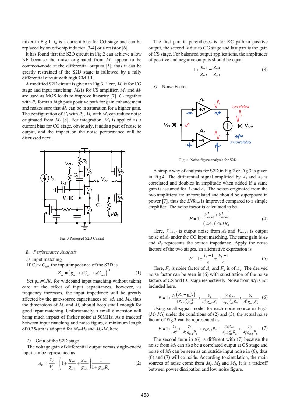
mixer in Fig.1.Ig is a current bias for CG stage and can be The first part in parentheses is for RC path to positive replaced by an off-chip inductor [3-4]or a resistor [6]. output,the second is due to CG stage and last part is the gain It has found that the S2D circuit in Fig.2 can achieve a low of CS stage.For balanced output applications,the amplitudes NF because the noise originated from M appear to be of positive and negative outputs should be equal common-mode at the differential outputs [5],thus it can be 1+8ml=8m4 greatly restrained if the S2D stage is followed by a fully (3) 8m2 8ms differential circuit with high CMRR. A modified S2D circuit is given in Fig.3.Here,M is for CG 3) Noise Factor stage and input matching,M is for CS amplifier.M2 and Ms are used as MOS loads to improve linearity [7].C,together with R,forms a high pass positive path for gain enhancement and makes sure that M can be in saturation for a higher gain. correlated The configuration of C,with R,M with M,can reduce noise originated from M [8].For integration,M;is applied as a current bias for CG stage,obviously,it adds a part of noise to Vn☒ ☒Vout output,and the impact on the noise performance will be discussed next. uncorrelated Fig.4 Noise figure analysis for S2D VB. A simple way of analysis for S2D in Fig.2 or Fig.3 is given in Fig.4.The differential signal amplified by A,and A2 is correlated and doubles in amplitude when added if a same gain is assumed for A,and 42.The noises originated from the Vn☒ M two amplifiers are uncorrelated and should be superposed in power [7],thus the SNRo is improved compared to a simple amplifier.The noise factor is calculated to be VB F=14+四运 (4) (24)4kTR Here,Vn is output noise from A and Vun is output Fig.3 Proposed S2D Circuit noise of 42 under the CG input matching.The same gain is Ar and Rs represents the source impedance.Apply the noise B.Performance Analysis factors of the two stages,an alternative expression is 1)Input matching F=1+F-1+E-1 (5) 44 If C>C.the input impedance of the S2D is Here,F,is noise factor of A,and F,is ofA2.The derived Z=(8m+sC+sCn)月 (1) noise factor can be seen in(6)with substitution of the noise Set gm=1/Rs for wideband input matching without taking factors of CS and CG stage respectively.Noise from M;is not care of the effect of input capacitances,however,as included here. frequency increases,the input impedance will be greatly affected by the gate-source capacitances of M and M,thus F=1+(B-8 ++8m4+ Y5(6) 4Rs Aigml AgmaRs ArgisRs gmsRs the dimensions of M,and M,should keep small enough for good input matching.Unfortunately,a small dimension will Using small-signal model for each noise source in Fig.3 bring much impact of flicker noise at 50MHz.As a tradeoff (M-Ms)under the conditions of (2)and (3),the actual noise factor of Fig.3 can be represented as between input matching and noise figure,a minimum length of 0.35-um is adopted for M-M2 and M-Ms here. +令+安gR+%8风+ F=1+ Y2 (7) ArgmsRs ArgmsRs 2)Gain of the S2D stage The second term in (6)is different with (7)because the The voltage gain of differential output versus single-ended noise from M,can also be a correlated output at CS stage and input can be represented as noise of M:can be seen as an outside input noise in (6),thus =1+8m+84月 (6)and(7)will coincide.According to simulation,the main Ay=- (2) sources of noise come from M.M,and M,it is a tradeoff V gm2 gms)1+gmRs between power dissipation and low noise figure. 458mixer in Fig.1. IB is a current bias for CG stage and can be replaced by an off-chip inductor [3-4] or a resistor [6]. It has found that the S2D circuit in Fig.2 can achieve a low NF because the noise originated from M1 appear to be common-mode at the differential outputs [5], thus it can be greatly restrained if the S2D stage is followed by a fully differential circuit with high CMRR. A modified S2D circuit is given in Fig.3. Here, M1 is for CG stage and input matching, M4 is for CS amplifier. M2 and M5 are used as MOS loads to improve linearity [7]. C1 together with R1 forms a high pass positive path for gain enhancement and makes sure that M1 can be in saturation for a higher gain. The configuration of C1 with R1, M1 with M2 can reduce noise originated from M1 [8]. For integration, M3 is applied as a current bias for CG stage, obviously, it adds a part of noise to output, and the impact on the noise performance will be discussed next. Fig. 3 Proposed S2D Circuit B. Performance Analysis 1) Input matching If C3>>Cgs1, the input impedance of the S2D is
1 Z g sC sC in m gs gs 114 (1) Set gm1=1/RS for wideband input matching without taking care of the effect of input capacitances, however, as frequency increases, the input impedance will be greatly affected by the gate-source capacitances of M1 and M4, thus the dimensions of M1 and M4 should keep small enough for good input matching. Unfortunately, a small dimension will bring much impact of flicker noise at 50MHz. As a tradeoff between input matching and noise figure, a minimum length of 0.35-ȝm is adopted for M1-M2 and M4-M5 here. 2) Gain of the S2D stage The voltage gain of differential output versus single-ended input can be represented as 1 4 25 1 1 1 1 d mm V s m m mS V gg A V g g gR § · ¨ ¸ © ¹ (2) The first part in parentheses is for RC path to positive output, the second is due to CG stage and last part is the gain of CS stage. For balanced output applications, the amplitudes of positive and negative outputs should be equal 1 4 2 5 1 m m m m g g g g (3) 3) Noise Factor Fig. 4 Noise figure analysis for S2D A simple way of analysis for S2D in Fig.2 or Fig.3 is given in Fig.4. The differential signal amplified by A1 and A2 is correlated and doubles in amplitude when added if a same gain is assumed for A1 and A2. The noises originated from the two amplifiers are uncorrelated and should be superposed in power [7], thus the SNRout is improved compared to a simple amplifier. The noise factor is calculated to be
2 2 ,1 ,2 2 1 2 4 out n out n V S V V F A kTR (4) Here, Vout,n1 is output noise from A1 and Vout,n2 is output noise of A2 under the CG input matching. The same gain is AV and RS represents the source impedance. Apply the noise factors of the two stages, an alternative expression is 1 2 1 1 1 4 4 F F F (5) Here, F1 is noise factor of A1 and F2 is of A2. The derived noise factor can be seen in (6) with substitution of the noise factors of CS and CG stage respectively. Noise from M3 is not included here.
2 1 1 2 2 44 5 21 2 2 2 12 5 5 1 4 S m m SV m V m S V m S V m S R g g F RAg Ag R Ag R Ag R J J J J (6) Using small-signal model for each noise source in Fig.3 (M1-M5) under the conditions of (2) and (3), the actual noise factor of Fig.3 can be represented as 1 2 44 5 22 2 2 3 3 2 55 1 m m S V Vm S Vm S Vm S g F gR A Ag R Ag R Ag R J J J J J (7) The second term in (6) is different with (7) because the noise from M1 can also be a correlated output at CS stage and noise of M3 can be seen as an outside input noise in (6), thus (6) and (7) will coincide. According to simulation, the main sources of noise come from M4, M2 and M3, it is a tradeoff between power dissipation and low noise figure. 458