正在加载图片...
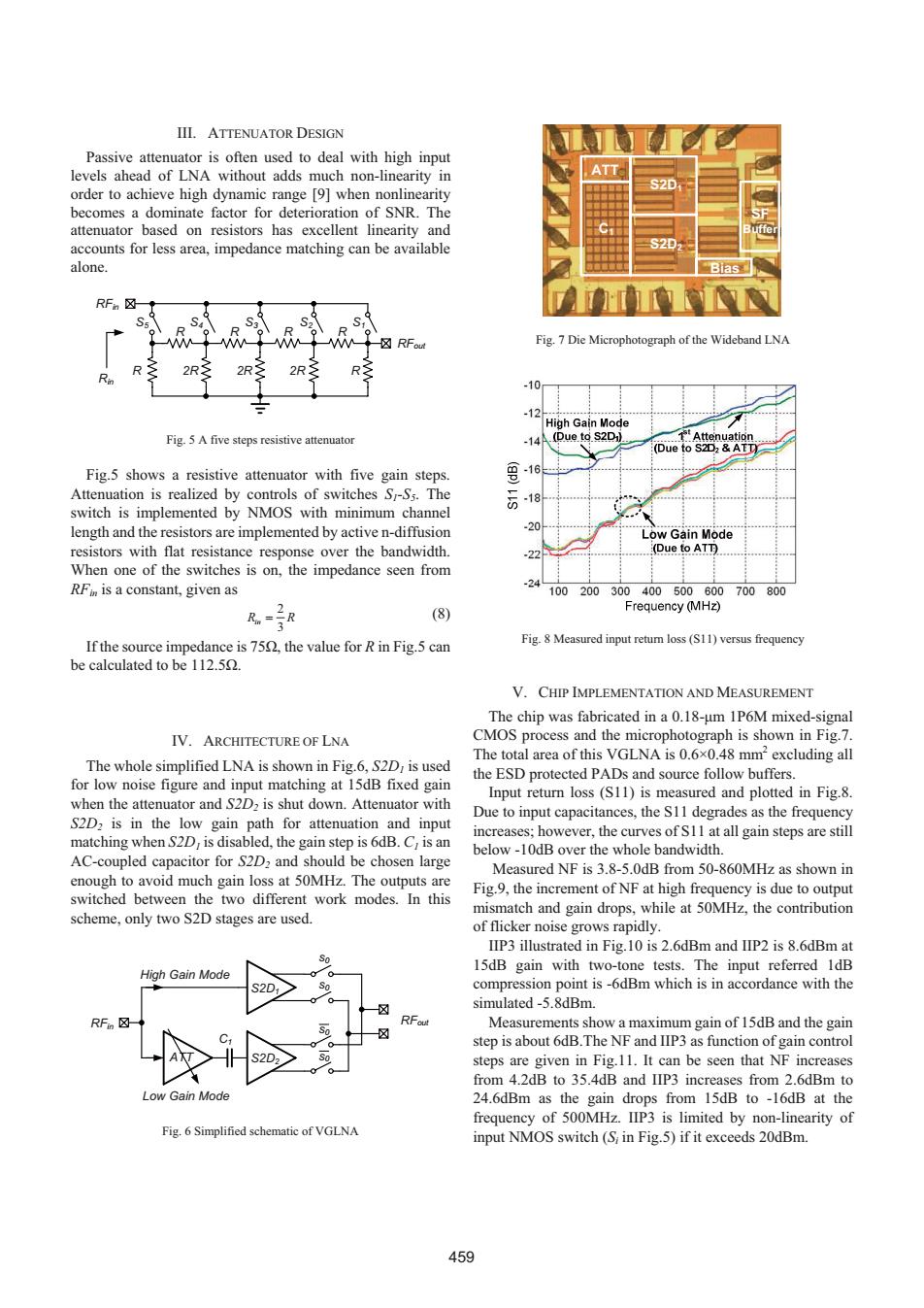
III.ATTENUATOR DESIGN Passive attenuator is often used to deal with high input levels ahead of LNA without adds much non-linearity in order to achieve high dynamic range [9]when nonlinearity becomes a dominate factor for deterioration of SNR.The attenuator based on resistors has excellent linearity and accounts for less area,impedance matching can be available alone. RFn☒ ☒RF Fig.7 Die Microphotograph of the Wideband LNA R 2R 2只 2 -10 -12 High Gain Mode Fig.5 A five steps resistive attenuator -14 (Due to S2Dj) 1Attenuation (Due to S2D2&ATT) Fig.5 shows a resistive attenuator with five gain steps. -16 Attenuation is realized by controls of switches S-Ss.The -18 switch is implemented by NMOS with minimum channel length and the resistors are implemented by active n-diffusion 20 Low Gain Mode resistors with flat resistance response over the bandwidth. (Due to ATT When one of the switches is on,the impedance seen from RFi is a constant,given as -24 100200300400500600700800 R.R (8) Frequency (MHz) If the source impedance is 750,the value for R in Fig.5 can Fig.8 Measured input retum loss(S11)versus frequency be calculated to be 112.50. V.CHIP IMPLEMENTATION AND MEASUREMENT The chip was fabricated in a 0.18-um 1P6M mixed-signal IV.ARCHITECTURE OF LNA CMOS process and the microphotograph is shown in Fig.7. The total area of this VGLNA is 0.6x0.48 mm2 excluding all The whole simplified LNA is shown in Fig.6,S2D,is used the ESD protected PADs and source follow buffers. for low noise figure and input matching at 15dB fixed gain Input return loss(S11)is measured and plotted in Fig.8 when the attenuator and S2D2 is shut down.Attenuator with Due to input capacitances,the S11 degrades as the frequency S2D2 is in the low gain path for attenuation and input matching when S2D,is disabled,the gain step is 6dB.C,is an increases;however,the curves of S11 at all gain steps are still below-10dB over the whole bandwidth. AC-coupled capacitor for S2D2 and should be chosen large Measured NF is 3.8-5.0dB from 50-860MHz as shown in enough to avoid much gain loss at 50MHz.The outputs are Fig.9,the increment of NF at high frequency is due to output switched between the two different work modes.In this scheme,only two S2D stages are used. mismatch and gain drops,while at 50MHz,the contribution of flicker noise grows rapidly. IIP3 illustrated in Fig.10 is 2.6dBm and IIP2 is 8.6dBm at 15dB gain with two-tone tests.The input referred 1dB High Gain Mode compression point is-6dBm which is in accordance with the simulated-5.8dBm. RFn☒ Measurements show a maximum gain of 15dB and the gain step is about 6dB.The NF and IIP3 as function of gain control steps are given in Fig.11.It can be seen that NF increases from 4.2dB to 35.4dB and IIP3 increases from 2.6dBm to Low Gain Mode 24.6dBm as the gain drops from 15dB to -16dB at the frequency of 500MHz.IIP3 is limited by non-linearity of Fig.6 Simplified schematic of VGLNA input NMOS switch(S in Fig.5)if it exceeds 20dBm. 459III. ATTENUATOR DESIGN Passive attenuator is often used to deal with high input levels ahead of LNA without adds much non-linearity in order to achieve high dynamic range [9] when nonlinearity becomes a dominate factor for deterioration of SNR. The attenuator based on resistors has excellent linearity and accounts for less area, impedance matching can be available alone. RFout R R R R R R 2R 2R 2R S5 S4 S3 S2 S1 RFin Rin Fig. 5 A five steps resistive attenuator Fig.5 shows a resistive attenuator with five gain steps. Attenuation is realized by controls of switches S1-S5. The switch is implemented by NMOS with minimum channel length and the resistors are implemented by active n-diffusion resistors with flat resistance response over the bandwidth. When one of the switches is on, the impedance seen from RFin is a constant, given as 2 3 Rin R (8) If the source impedance is 75ȍ, the value for R in Fig.5 can be calculated to be 112.5ȍ. IV. ARCHITECTURE OF LNA The whole simplified LNA is shown in Fig.6, S2D1 is used for low noise figure and input matching at 15dB fixed gain when the attenuator and S2D2 is shut down. Attenuator with S2D2 is in the low gain path for attenuation and input matching when S2D1 is disabled, the gain step is 6dB. C1 is an AC-coupled capacitor for S2D2 and should be chosen large enough to avoid much gain loss at 50MHz. The outputs are switched between the two different work modes. In this scheme, only two S2D stages are used. RFin RFout S2D1 ATT S2D2 C1 High Gain Mode Low Gain Mode s0 s0 s0 s0 Fig. 6 Simplified schematic of VGLNA ATT C1 S2D2 S2D1 SF Buffer Bias Fig. 7 Die Microphotograph of the Wideband LNA Fig. 8 Measured input return loss (S11) versus frequency V. CHIP IMPLEMENTATION AND MEASUREMENT The chip was fabricated in a 0.18-ȝm 1P6M mixed-signal CMOS process and the microphotograph is shown in Fig.7. The total area of this VGLNA is 0.6×0.48 mm2 excluding all the ESD protected PADs and source follow buffers. Input return loss (S11) is measured and plotted in Fig.8. Due to input capacitances, the S11 degrades as the frequency increases; however, the curves of S11 at all gain steps are still below -10dB over the whole bandwidth. Measured NF is 3.8-5.0dB from 50-860MHz as shown in Fig.9, the increment of NF at high frequency is due to output mismatch and gain drops, while at 50MHz, the contribution of flicker noise grows rapidly. IIP3 illustrated in Fig.10 is 2.6dBm and IIP2 is 8.6dBm at 15dB gain with two-tone tests. The input referred 1dB compression point is -6dBm which is in accordance with the simulated -5.8dBm. Measurements show a maximum gain of 15dB and the gain step is about 6dB.The NF and IIP3 as function of gain control steps are given in Fig.11. It can be seen that NF increases from 4.2dB to 35.4dB and IIP3 increases from 2.6dBm to 24.6dBm as the gain drops from 15dB to -16dB at the frequency of 500MHz. IIP3 is limited by non-linearity of input NMOS switch (Si in Fig.5) if it exceeds 20dBm. 459