正在加载图片...
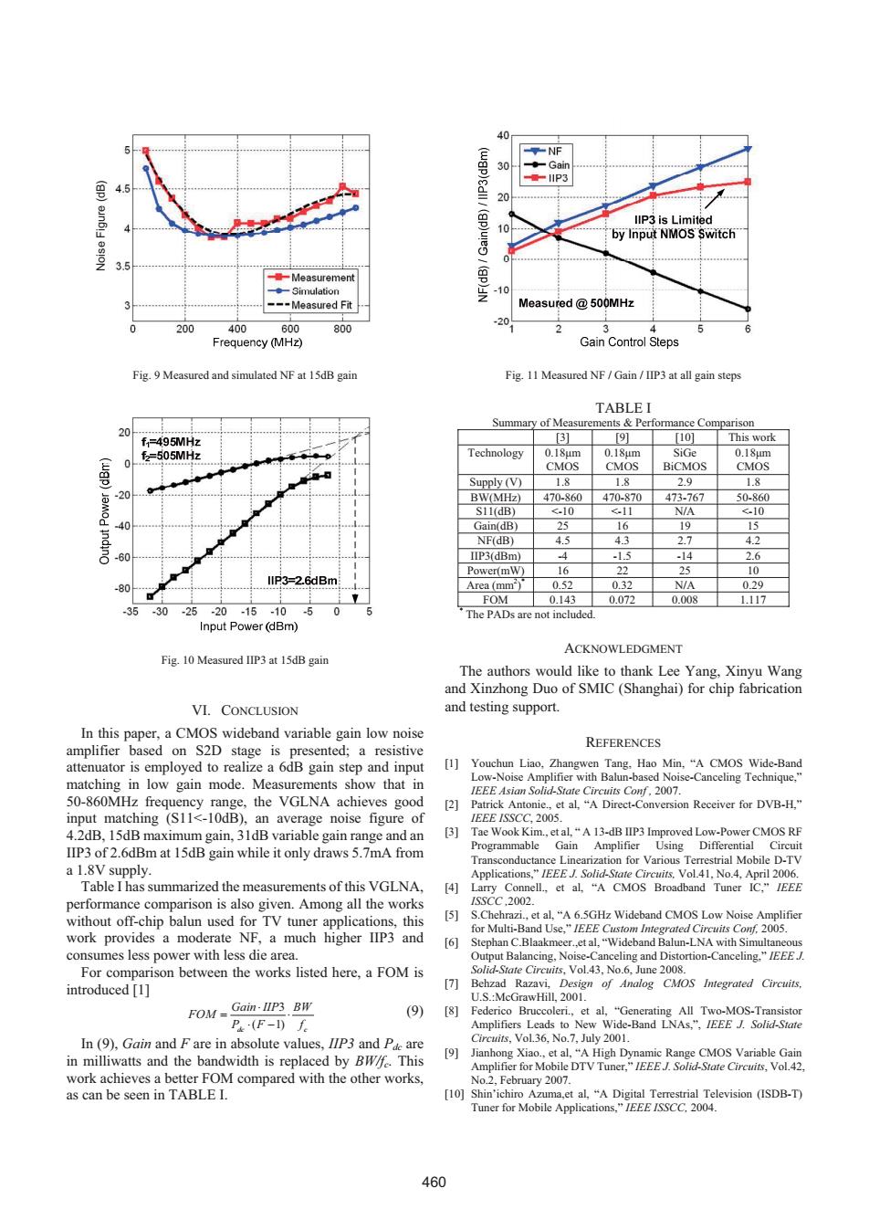
40 NF ◆-Gain 01P3 49 20 IIP3 is Limited 10 by Input NMOS Switch 量-Measurement -Simulation 10 -Measured Fit Measured 500MHz 20 200 400 600 800 d Frequency (MHz) Gain Control Steps Fig.9 Measured and simulated NF at 15dB gain Fig.11 Measured NF/Gain IIP3 at all gain steps TABLEI Summary of Measurements Performance Comparison f=495MHz [3] 9] [101 This work =505MHz Technology 0.18um 0.18um SiGe 0.18μm 0 CMOS CMOS BiCMOS CMOS Supply (V) 1.8 1.8 2.9 1.8 20 BW(MHz) 470-860 470.870 473.767 50-860 S11(dB) <.10 11 N/A <-10 40 Gain(dB) 25 16 19 15 NF(dB) 4.5 4.3 2.7 4.2 -60 IIP3(dBm) 4 -1.5 -14 2.6 Power(mW) 16 22 25 10 IIP3=2.6dBm 0 Area (mm) 0.52 0.32 N/A 0.29 FOM 0.143 0.072 0008 1.117 .35 -30-25-20-15-10-5 The PADs are not included Input Power (dBm) ACKNOWLEDGMENT Fig.10 Measured IIP3 at 15dB gain The authors would like to thank Lee Yang,Xinyu Wang and Xinzhong Duo of SMIC (Shanghai)for chip fabrication VI.CONCLUSION and testing support. In this paper,a CMOS wideband variable gain low noise REFERENCES amplifier based on S2D stage is presented;a resistive attenuator is employed to realize a 6dB gain step and input [1]Youchun Liao,Zhangwen Tang.Hao Min."A CMOS Wide-Band matching in low gain mode.Measurements show that in Low-Noise Amplifier with Balun-based Noise-Canceling Technique," IEEE Asian Solid-State Circuits Conf,2007. 50-860MHz frequency range,the VGLNA achieves good [2] Patrick Antonie.,et al,"A Direct-Conversion Receiver for DVB-H," input matching (S11<-10dB),an average noise figure of IEEE ISSCC.2005. 4.2dB.15dB maximum gain,31dB variable gain range and an [3] Tae Wook Kim.,et al,"A 13-dB IIP3 Improved Low-Power CMOS RF IIP3 of 2.6dBm at 15dB gain while it only draws 5.7mA from Programmable Gain Amplifier Using Differential Circuit Transconductance Linearization for Various Terrestrial Mobile D-TV a 1.8V supply. Applications,"IEEE J.Solid-State Circuits,Vol.41,No.4,April 2006. Table I has summarized the measurements of this VGLNA. [4 Larry Connell.,et al,"A CMOS Broadband Tuner IC,"/EEE performance comparison is also given.Among all the works ISSCC,2002. without off-chip balun used for TV tuner applications,this [5] S.Chehrazi.,et al,"A 6.5GHz Wideband CMOS Low Noise Amplifier for Multi-Band Use,"IEEE Custom Integrated Circuits Conf,2005. work provides a moderate NF,a much higher IIP3 and [6] Stephan C.Blaakmeer.,et al,"Wideband Balun-LNA with Simultaneous consumes less power with less die area. Output Balancing,Noise-Canceling and Distortion-Canceling."IEEE For comparison between the works listed here,a FOM is Solid-State Circuits,Vol.43,No.6,June 2008. introduced [1] 7刀 Behzad Razavi,Design of Analog CMOS Integrated Circuits, FOM=Gain-IIP3 BW U.S.:McGrawHill,2001. (9) [8]Federico Bruccoleri.,et al,"Generating All Two-MOS-Transistor ΓP(F-)f Amplifiers Leads to New Wide-Band LNAs,",IEEE J.Solid-State In(9).Gain and F are in absolute values,IIP3 and Pde are Circuits,Vol.36.No.7,July 2001. [9] in milliwatts and the bandwidth is replaced by BWf.This Jianhong Xiao.,et al,"A High Dynamic Range CMOS Variable Gain Amplifier for Mobile DTV Tuner,"IEEE J.Solid-State Circuits,Vol.42, work achieves a better FOM compared with the other works, No.2.February 2007. as can be seen in TABLE I. [10]Shin'ichiro Azuma,et al,"A Digital Terrestrial Television (ISDB-T) Tuner for Mobile Applications,"IEEE /SSCC.2004. 4601RLVH)LJXUH
G%
Fig. 9 Measured and simulated NF at 15dB gain Fig. 10 Measured IIP3 at 15dB gain VI. CONCLUSION In this paper, a CMOS wideband variable gain low noise amplifier based on S2D stage is presented; a resistive attenuator is employed to realize a 6dB gain step and input matching in low gain mode. Measurements show that in 50-860MHz frequency range, the VGLNA achieves good input matching (S11<-10dB), an average noise figure of 4.2dB, 15dB maximum gain, 31dB variable gain range and an IIP3 of 2.6dBm at 15dB gain while it only draws 5.7mA from a 1.8V supply. Table I has summarized the measurements of this VGLNA, performance comparison is also given. Among all the works without off-chip balun used for TV tuner applications, this work provides a moderate NF, a much higher IIP3 and consumes less power with less die area. For comparison between the works listed here, a FOM is introduced [1] 3 ( 1) dc c Gain IIP BW FOM P F f (9) In (9), Gain and F are in absolute values, IIP3 and Pdc are in milliwatts and the bandwidth is replaced by BW/fc. This work achieves a better FOM compared with the other works, as can be seen in TABLE I. Fig. 11 Measured NF / Gain / IIP3 at all gain steps TABLE I Summary of Measurements & Performance Comparison [3] [9] [10] This work Technology 0.18ȝm CMOS 0.18ȝm CMOS SiGe BiCMOS 0.18ȝm CMOS Supply (V) 1.8 1.8 2.9 1.8 BW(MHz) 470-860 470-870 473-767 50-860 S11(dB) <-10 <-11 N/A <-10 Gain(dB) 25 16 19 15 NF(dB) 4.5 4.3 2.7 4.2 IIP3(dBm) -4 -1.5 -14 2.6 Power(mW) 16 22 25 10 Area (mm2 ) * 0.52 0.32 N/A 0.29 FOM 0.143 0.072 0.008 1.117 * The PADs are not included. ACKNOWLEDGMENT The authors would like to thank Lee Yang, Xinyu Wang and Xinzhong Duo of SMIC (Shanghai) for chip fabrication and testing support. REFERENCES [1] Youchun Liao, Zhangwen Tang, HaR 0LQ ³$ &026 :LGH%DQG /RZ1RLVH$PSOLILHUZLWK%DOXQEDVHG1RLVH&DQFHOLQJ7HFKQLTXH´ IEEE Asian Solid-State Circuits Conf , 2007. [2] 3DWULFN$QWRQLH HW DO ³$'LUHFW&RQYHUVLRQ5HFHLYHU IRU'9%+´ IEEE ISSCC, 2005. [3] 7DH:RRN.LPHWDO³$G%,,3,PSURYHG/RZ3RZHU&0265) Programmable Gain Amplifier Using Differential Circuit Transconductance Linearization for Various Terrestrial Mobile D-TV $SSOLFDWLRQV´IEEE J. Solid-State Circuits, Vol.41, No.4, April 2006. [4] /DUU\ &RQQHOO HW DO ³$ &026 %URDGEDQG 7XQHU ,&´ IEEE ISSCC ,2002. [5] 6&KHKUD]LHWDO³$*+]:Ldeband CMOS Low Noise Amplifier IRU0XOWL%DQG8VH´IEEE Custom Integrated Circuits Conf, 2005. [6] 6WHSKDQ&%ODDNPHHUHWDO³:LGHEDQG%DOXQ/1$ZLWK6LPXOWDQHRXV Output Balancing, Noise-CanceOLQJDQG'LVWRUWLRQ&DQFHOLQJ´IEEE J. Solid-State Circuits, Vol.43, No.6, June 2008. [7] Behzad Razavi, Design of Analog CMOS Integrated Circuits, U.S.:McGrawHill, 2001. [8] )HGHULFR %UXFFROHUL HW DO ³*HQHUDWLQJ $OO 7ZR0267UDQVLVWRU $PSOLILHUV /HDGV WR 1HZ :LGH%DQG /1$V´ IEEE J. Solid-State Circuits, Vol.36, No.7, July 2001. [9] -LDQKRQJ;LDRHWDO³$+LJK'\QDPLF5DQJH&0269DULDEOH*DLQ $PSOLILHUIRU0RELOH'797XQHU´IEEE J. Solid-State Circuits, Vol.42, No.2, February 2007. [10] 6KLQ¶LFKLUR $]XPDHW DO ³$ 'LJLWDO 7HUUHVWULDO 7HOHYLVLRQ
,6'%7
7XQHUIRU0RELOH$SSOLFDWLRQV´IEEE ISSCC, 2004. 460��������������������������������������������������������������������������������������������������������