正在加载图片...
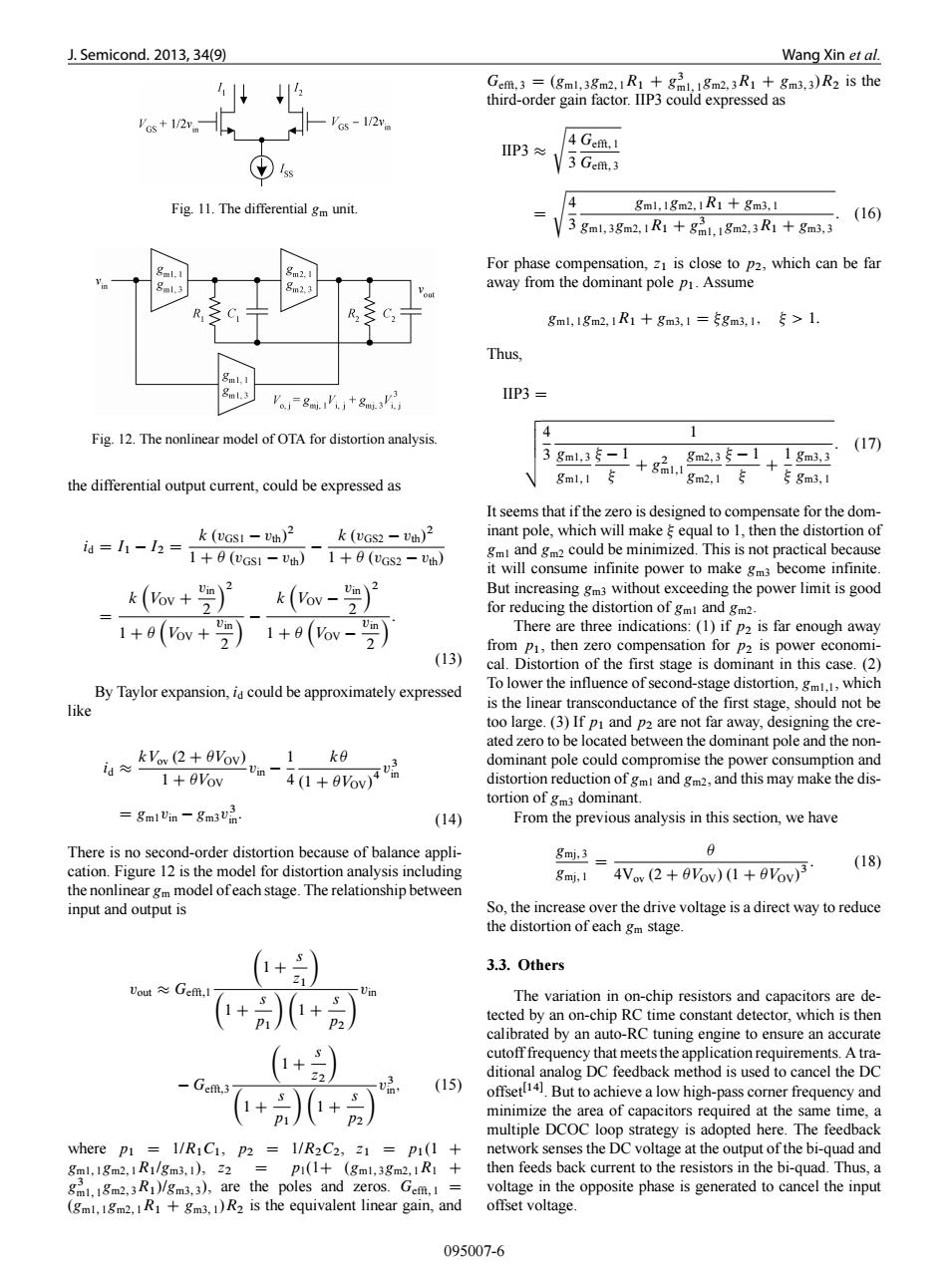
J.Semicond.2013,34(9) Wang Xin et al. Gem.3 =(gml,38m2.R1+g8m2.3R1+8m3,3)R2 is the third-order gain factor.IIP3 could expressed as 'cs-1/2w IP3≈ 4 Gem.1 13 Gemt,3 Fig.11.The differential gm unit. 4 gml,1gm2,1R1十gm3,1 √3gml,3gam2,1R1+g品,18m2,3R1+8m3,3 (16) For phase compensation,z is close to p2,which can be far m? away from the dominant pole pi.Assume 8ml,18m2,1R1+gm3,1=专gm3,1,5>1. Thus, 8ml.3 Vagm IIP3= Fig.12.The nonlinear model of OTA for distortion analysis. 1 3gml,35-1 8m2,35-1,1gm3,3 (17) the differential output current,could be expressed as 8ml,1专 +g品gm15 5gm3,1 It seems that if the zero is designed to compensate for the dom- k (vGSI -Uth)2 k (vGS2-Uth)2 inant pole,which will make equal to 1,then the distortion of ia=h-1h=1+9cs1-m-1+0(wGs2-w】 gmi and gm2 could be minimized.This is not practical because it will consume infinite power to make gm3 become infinite. (ov+ k(ow-》 But increasing gm3 without exceeding the power limit is good for reducing the distortion of gmi and gm2. 1+0(ov+罗)1+0(ov- There are three indications:(1)if p2 is far enough away from p1,then zero compensation for p2 is power economi- (13) cal.Distortion of the first stage is dominant in this case.(2) By Taylor expansion,id could be approximately expressed To lower the influence of second-stage distortion,gmi.1,which like is the linear transconductance of the first stage,should not be too large.(3)If pi and p2 are not far away,designing the cre- a≈k.2+6ou-1ke ated zero to be located between the dominant pole and the non- 40+9row号 dominant pole could compromise the power consumption and 1+0Vov distortion reduction of gmi and gm2,and this may make the dis- tortion of gm3 dominant. =gmlVin-gmV (14) From the previous analysis in this section,we have There is no second-order distortion because of balance appli- 8mj,3 cation.Figure 12 is the model for distortion analysis including 8mj,1 4Vv(2+9ov)1+9ov)31 (18) the nonlinear gm model ofeach stage.The relationship between input and output is So,the increase over the drive voltage is a direct way to reduce the distortion of each gm stage. + 3.3.Others vout≈Gem, +)+) The variation in on-chip resistors and capacitors are de- tected by an on-chip RC time constant detector,which is then calibrated by an auto-RC tuning engine to ensure an accurate (+) cutoff frequency that meets the application requirements.A tra- ditional analog DC feedback method is used to cancel the DC -Gef.3 (15) +)+) offset14).But to achieve a low high-pass corner frequency and minimize the area of capacitors required at the same time,a multiple DCOC loop strategy is adopted here.The feedback Where p1 1/R1C1,p2 1/R2C2,21 p1(1 network senses the DC voltage at the output of the bi-quad and gm1,18m2,1 R1/gm3,1),Z2 =p1(1+(gml,38m2,1R1+ then feeds back current to the resistors in the bi-quad.Thus,a gm1.18m2.3R1)/gm3.3),are the poles and zeros.Gem.1= voltage in the opposite phase is generated to cancel the input (gm1,18m2,1R1+gm3.1)R2 is the equivalent linear gain,and offset voltage 095007-6J. Semicond. 2013, 34(9) Wang Xin et al. Fig. 11. The differential gm unit. Fig. 12. The nonlinear model of OTA for distortion analysis. the differential output current, could be expressed as id D I1 I2 D k .vGS1 vth/ 2 1 C .vGS1 vth/ k .vGS2 vth/ 2 1 C .vGS2 vth/ D k VOV C vin 2 2 1 C VOV C vin 2 k VOV vin 2 2 1 C VOV vin 2 : (13) By Taylor expansion, id could be approximately expressed like id kVov .2 C VOV/ 1 C VOV vin 1 4 k .1 C VOV/ 4 v 3 in D gm1vin gm3v 3 in: (14) There is no second-order distortion because of balance application. Figure 12 is the model for distortion analysis including the nonlinear gm model of each stage. The relationship between input and output is vout Gefft;1 1 C s z1 1 C s p1 1 C s p2 vin Gefft;3 1 C s z2 1 C s p1 1 C s p2 v 3 in; (15) where p1 D 1/R1C1, p2 D 1/R2C2, z1 D p1.1 C gm1; 1gm2; 1R1/gm3; 1/, z2 D p1(1C (gm1; 3gm2; 1R1 C g 3 m1; 1 gm2; 3R1//gm3; 3/, are the poles and zeros. Gefft; 1 D (gm1; 1gm2; 1R1 C gm3; 1/R2 is the equivalent linear gain, and Gefft; 3 D (gm1; 3gm2; 1R1 C g 3 m1; 1 gm2; 3R1 C gm3; 3/R2 is the third-order gain factor. IIP3 could expressed as IIP3 s 4 3 Gefft; 1 Gefft; 3 D s 4 3 gm1; 1gm2; 1R1 C gm3; 1 gm1; 3gm2; 1R1 C g 3 m1; 1 gm2; 3R1 C gm3; 3 : (16) For phase compensation, z1 is close to p2, which can be far away from the dominant pole p1. Assume gm1; 1gm2; 1R1 C gm3; 1 D gm3; 1; > 1: Thus, IIP3 D vuuut 4 3 1 gm1; 3 gm1; 1 1 C g 2 m1;1 gm2; 3 gm2; 1 1 C 1 gm3; 3 gm3; 1 : (17) It seems that if the zero is designed to compensate for the dominant pole, which will make equal to 1, then the distortion of gm1 and gm2 could be minimized. This is not practical because it will consume infinite power to make gm3 become infinite. But increasing gm3 without exceeding the power limit is good for reducing the distortion of gm1 and gm2. There are three indications: (1) if p2 is far enough away from p1, then zero compensation for p2 is power economical. Distortion of the first stage is dominant in this case. (2) To lower the influence of second-stage distortion, gm1;1, which is the linear transconductance of the first stage, should not be too large. (3) If p1 and p2 are not far away, designing the created zero to be located between the dominant pole and the nondominant pole could compromise the power consumption and distortion reduction of gm1 and gm2, and this may make the distortion of gm3 dominant. From the previous analysis in this section, we have gmj; 3 gmj; 1 D 4Vov .2 C VOV/ .1 C VOV/ 3 : (18) So, the increase over the drive voltage is a direct way to reduce the distortion of each gm stage. 3.3. Others The variation in on-chip resistors and capacitors are detected by an on-chip RC time constant detector, which is then calibrated by an auto-RC tuning engine to ensure an accurate cutoff frequency that meets the application requirements. A traditional analog DC feedback method is used to cancel the DC offsetŒ14. But to achieve a low high-pass corner frequency and minimize the area of capacitors required at the same time, a multiple DCOC loop strategy is adopted here. The feedback network senses the DC voltage at the output of the bi-quad and then feeds back current to the resistors in the bi-quad. Thus, a voltage in the opposite phase is generated to cancel the input offset voltage. 095007-6