正在加载图片...
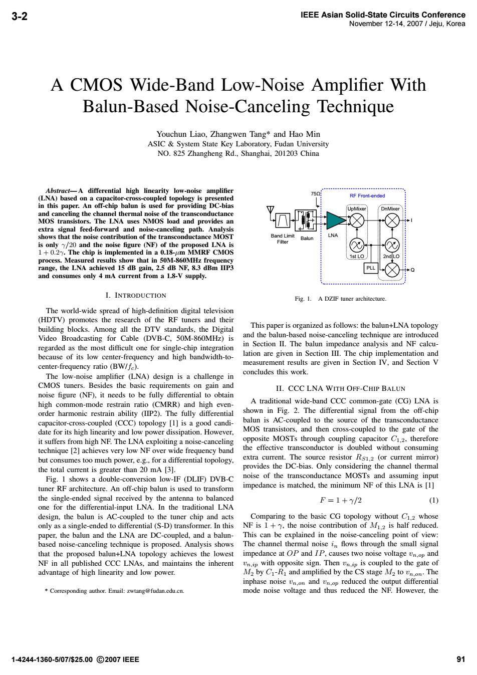
3-2 IEEE Asian Solid-State Circuits Conference November 12-14.2007/Jeju,Korea A CMOS Wide-Band Low-Noise Amplifier With Balun-Based Noise-Canceling Technique Youchun Liao,Zhangwen Tang*and Hao Min ASIC System State Key Laboratory,Fudan University NO.825 Zhangheng Rd.,Shanghai,201203 China Abstract-A differential high linearity low-noise amplifier (LNA)based on a capacitor-cross-coupled topology is presented RF Front-ended in this paper.An off-chip balun is used for providing DC-bias UpMixer and canceling the channel thermal noise of the transconductance MOS transistors.The LNA uses NMOS load and provides an extra signal feed-forward and noise-canceling path.Analysis shows that the noise contribution of the transconductance MOST Band Limit Balun LNA is only yy/20 and the noise figure (NF)of the proposed LNA is 1+0.2.The chip is implemented in a 0.18-um MMRF CMOS process.Measured results show that in 50M-860MHz frequency range,the LNA achieved 15 dB gain,2.5 dB NF,8.3 dBm IIP3 and consumes only 4 mA current from a 1.8-V supply. I.INTRODUCTION Fig.1.A DZIF tuner architecture. The world-wide spread of high-definition digital television (HDTV)promotes the research of the RF tuners and their building blocks.Among all the DTV standards,the Digital This paper is organized as follows:the balun+LNA topology Video Broadcasting for Cable (DVB-C,50M-860MHz)is and the balun-based noise-canceling technique are introduced regarded as the most difficult one for single-chip integration in Section II.The balun impedance analysis and NF calcu- because of its low center-frequency and high bandwidth-to- lation are given in Section III.The chip implementation and center-frequency ratio (BW/fe). measurement results are given in Section IV,and Section V The low-noise amplifier (LNA)design is a challenge in concludes this work. CMOS tuners.Besides the basic requirements on gain and II.CCC LNA WITH OFF-CHIP BALUN noise figure (NF),it needs to be fully differential to obtain high common-mode restrain ratio (CMRR)and high even- A traditional wide-band CCC common-gate (CG)LNA is order harmonic restrain ability (IIP2).The fully differential shown in Fig.2.The differential signal from the off-chip capacitor-cross-coupled (CCC)topology [1]is a good candi- balun is AC-coupled to the source of the transconductance date for its high linearity and low power dissipation.However, MOS transistors,and then cross-coupled to the gate of the it suffers from high NF.The LNA exploiting a noise-canceling opposite MOSTs through coupling capacitor C1.2.therefore technique [2]achieves very low NF over wide frequency band the effective transconductor is doubled without consuming but consumes too much power,e.g.,for a differential topology, extra current.The source resistor Rs1.2 (or current mirror) the total current is greater than 20 mA [3]. provides the DC-bias.Only considering the channel thermal Fig.1 shows a double-conversion low-IF (DLIF)DVB-C noise of the transconductance MOSTs and assuming input tuner RF architecture.An off-chip balun is used to transform impedance is matched,the minimum NF of this LNA is [1] the single-ended signal received by the antenna to balanced F=1+Y/2 (1) one for the differential-input LNA.In the traditional LNA design,the balun is AC-coupled to the tuner chip and acts Comparing to the basic CG topology without C1.2 whose only as a single-ended to differential(S-D)transformer.In this NF is 1+,the noise contribution of M.2 is half reduced. paper,the balun and the LNA are DC-coupled,and a balun- This can be explained in the noise-canceling point of view: based noise-canceling technique is proposed.Analysis shows The channel thermal noise in flows through the small signal that the proposed balun+LNA topology achieves the lowest impedance at OP and IP,causes two noise voltagen and NF in all published CCC LNAs,and maintains the inherent Un.ip with opposite sign.Then Un.ip is coupled to the gate of advantage of high linearity and low power. M2 by C1-R and amplified by the CS stage M2 to vn.on.The inphase noise vn.n and vn.p reduced the output differential Corresponding author.Email:zwtang@fudan.edu.cn. mode noise voltage and thus reduced the NF.However,the 1-4244-1360-5/07/s25.00©20071EEE 91A CMOS Wide-Band Low-Noise Amplifier With Balun-Based Noise-Canceling Technique Youchun Liao, Zhangwen Tang* and Hao Min ASIC & System State Key Laboratory, Fudan University NO. 825 Zhangheng Rd., Shanghai, 201203 China Abstract— A differential high linearity low-noise amplifier (LNA) based on a capacitor-cross-coupled topology is presented in this paper. An off-chip balun is used for providing DC-bias and canceling the channel thermal noise of the transconductance MOS transistors. The LNA uses NMOS load and provides an extra signal feed-forward and noise-canceling path. Analysis shows that the noise contribution of the transconductance MOST is only γ/20 and the noise figure (NF) of the proposed LNA is 1+0.2γ. The chip is implemented in a 0.18-μm MMRF CMOS process. Measured results show that in 50M-860MHz frequency range, the LNA achieved 15 dB gain, 2.5 dB NF, 8.3 dBm IIP3 and consumes only 4 mA current from a 1.8-V supply. I. INTRODUCTION The world-wide spread of high-definition digital television (HDTV) promotes the research of the RF tuners and their building blocks. Among all the DTV standards, the Digital Video Broadcasting for Cable (DVB-C, 50M-860MHz) is regarded as the most difficult one for single-chip integration because of its low center-frequency and high bandwidth-tocenter-frequency ratio (BW/fc). The low-noise amplifier (LNA) design is a challenge in CMOS tuners. Besides the basic requirements on gain and noise figure (NF), it needs to be fully differential to obtain high common-mode restrain ratio (CMRR) and high evenorder harmonic restrain ability (IIP2). The fully differential capacitor-cross-coupled (CCC) topology [1] is a good candidate for its high linearity and low power dissipation. However, it suffers from high NF. The LNA exploiting a noise-canceling technique [2] achieves very low NF over wide frequency band but consumes too much power, e.g., for a differential topology, the total current is greater than 20 mA [3]. Fig. 1 shows a double-conversion low-IF (DLIF) DVB-C tuner RF architecture. An off-chip balun is used to transform the single-ended signal received by the antenna to balanced one for the differential-input LNA. In the traditional LNA design, the balun is AC-coupled to the tuner chip and acts only as a single-ended to differential (S-D) transformer. In this paper, the balun and the LNA are DC-coupled, and a balunbased noise-canceling technique is proposed. Analysis shows that the proposed balun+LNA topology achieves the lowest NF in all published CCC LNAs, and maintains the inherent advantage of high linearity and low power. * Corresponding author. Email: zwtang@fudan.edu.cn. PLL Band Limit Filter LNA 75ȍ UpMixer DnMixer 1st LO I Q RF Front-ended Balun 2nd LO Fig. 1. A DZIF tuner architecture. This paper is organized as follows: the balun+LNA topology and the balun-based noise-canceling technique are introduced in Section II. The balun impedance analysis and NF calculation are given in Section III. The chip implementation and measurement results are given in Section IV, and Section V concludes this work. II. CCC LNA WITH OFF-CHIP BALUN A traditional wide-band CCC common-gate (CG) LNA is shown in Fig. 2. The differential signal from the off-chip balun is AC-coupled to the source of the transconductance MOS transistors, and then cross-coupled to the gate of the opposite MOSTs through coupling capacitor C1,2, therefore the effective transconductor is doubled without consuming extra current. The source resistor RS1,2 (or current mirror) provides the DC-bias. Only considering the channel thermal noise of the transconductance MOSTs and assuming input impedance is matched, the minimum NF of this LNA is [1] F =1+ γ/2 (1) Comparing to the basic CG topology without C1,2 whose NF is 1 + γ, the noise contribution of M1,2 is half reduced. This can be explained in the noise-canceling point of view: The channel thermal noise in flows through the small signal impedance at OP and IP, causes two noise voltage vn,op and vn,ip with opposite sign. Then vn,ip is coupled to the gate of M2 by C1-R1 and amplified by the CS stage M2 to vn,on. The inphase noise vn,on and vn,op reduced the output differential mode noise voltage and thus reduced the NF. However, the IEEE Asian Solid-State Circuits Conference 1-4244-1360-5/07/$25.00 2007 IEEE November 12-14, 2007 / Jeju, Korea 3-2 91