正在加载图片...
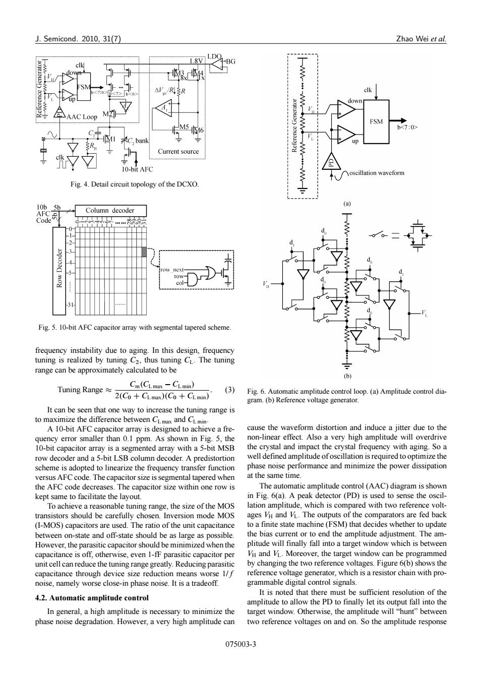
J.Semicond.2010,31(7) Zhao Wei et al. L8V]LDO △R3R clk down AAC Loop M2 M546 FSM C左I 米C,bank Current source “7☑ 10-bit AFC oscillation waveform Fig.4.Detail circuit topology of the DCXO. (a 10b 5b AFC Column decoder Code -2 4 col- Fig 5.10-bit AFC capacitor array with segmental tapered scheme. frequency instability due to aging.In this design,frequency tuning is realized by tuning C2,thus tuning CL.The tuning range can be approximately calculated to be (b) Tuning Range≈ Cm(CLmax-CLmin) (3) 2(Co+CLmax)(Co+CLmin) Fig.6.Automatic amplitude control loop.(a)Amplitude control dia- gram.(b)Reference voltage generator. It can be seen that one way to increase the tuning range is to maximize the difference between CLmax and CLmin. A 10-bit AFC capacitor array is designed to achieve a fre- cause the waveform distortion and induce a jitter due to the quency error smaller than 0.1 ppm.As shown in Fig.5,the non-linear effect.Also a very high amplitude will overdrive 10-bit capacitor array is a segmented array with a 5-bit MSB the crystal and impact the crystal frequency with aging.So a row decoder and a 5-bit LSB column decoder.A predistortion well defined amplitude ofoscillation is required to optimize the scheme is adopted to linearize the frequency transfer function phase noise performance and minimize the power dissipation versus AFC code.The capacitor size is segmental tapered when at the same time. the AFC code decreases.The capacitor size within one row is The automatic amplitude control (AAC)diagram is shown kept same to facilitate the layout. in Fig.6(a).A peak detector(PD)is used to sense the oscil- To achieve a reasonable tuning range,the size of the MOS lation amplitude,which is compared with two reference volt- transistors should be carefully chosen.Inversion mode MOS ages VH and V.The outputs of the comparators are fed back (I-MOS)capacitors are used.The ratio of the unit capacitance to a finite state machine(FSM)that decides whether to update between on-state and off-state should be as large as possible. the bias current or to end the amplitude adjustment.The am- However,the parasitic capacitor should be minimized when the plitude will finally fall into a target window which is between capacitance is off,otherwise,even 1-fF parasitic capacitor per VH and V.Moreover,the target window can be programmed unit cell can reduce the tuning range greatly.Reducing parasitic by changing the two reference voltages.Figure 6(b)shows the capacitance through device size reduction means worse 1/f reference voltage generator,which is a resistor chain with pro- noise,namely worse close-in phase noise.It is a tradeoff. grammable digital control signals. It is noted that there must be sufficient resolution of the 4.2.Automatic amplitude control amplitude to allow the PD to finally let its output fall into the In general,a high amplitude is necessary to minimize the target window.Otherwise,the amplitude will "hunt"between phase noise degradation.However,a very high amplitude can two reference voltages on and on.So the amplitude response 075003-3J. Semicond. 2010, 31(7) Zhao Wei et al. Fig. 4. Detail circuit topology of the DCXO. Fig. 5. 10-bit AFC capacitor array with segmental tapered scheme. frequency instability due to aging. In this design, frequency tuning is realized by tuning C2, thus tuning CL. The tuning range can be approximately calculated to be Tuning Range Cm.CL max CL min/ 2.C0 C CL max/.C0 C CL min/ : (3) It can be seen that one way to increase the tuning range is to maximize the difference between CL max and CL min. A 10-bit AFC capacitor array is designed to achieve a frequency error smaller than 0.1 ppm. As shown in Fig. 5, the 10-bit capacitor array is a segmented array with a 5-bit MSB row decoder and a 5-bit LSB column decoder. A predistortion scheme is adopted to linearize the frequency transfer function versus AFC code. The capacitor size is segmental tapered when the AFC code decreases. The capacitor size within one row is kept same to facilitate the layout. To achieve a reasonable tuning range, the size of the MOS transistors should be carefully chosen. Inversion mode MOS (I-MOS) capacitors are used. The ratio of the unit capacitance between on-state and off-state should be as large as possible. However, the parasitic capacitor should be minimized when the capacitance is off, otherwise, even 1-fF parasitic capacitor per unit cell can reduce the tuning range greatly. Reducing parasitic capacitance through device size reduction means worse 1/f noise, namely worse close-in phase noise. It is a tradeoff. 4.2. Automatic amplitude control In general, a high amplitude is necessary to minimize the phase noise degradation. However, a very high amplitude can Fig. 6. Automatic amplitude control loop. (a) Amplitude control diagram. (b) Reference voltage generator. cause the waveform distortion and induce a jitter due to the non-linear effect. Also a very high amplitude will overdrive the crystal and impact the crystal frequency with aging. So a well defined amplitude of oscillation is required to optimize the phase noise performance and minimize the power dissipation at the same time. The automatic amplitude control (AAC) diagram is shown in Fig. 6(a). A peak detector (PD) is used to sense the oscillation amplitude, which is compared with two reference voltages VH and VL. The outputs of the comparators are fed back to a finite state machine (FSM) that decides whether to update the bias current or to end the amplitude adjustment. The amplitude will finally fall into a target window which is between VH and VL. Moreover, the target window can be programmed by changing the two reference voltages. Figure 6(b) shows the reference voltage generator, which is a resistor chain with programmable digital control signals. It is noted that there must be sufficient resolution of the amplitude to allow the PD to finally let its output fall into the target window. Otherwise, the amplitude will “hunt” between two reference voltages on and on. So the amplitude response 075003-3