正在加载图片...
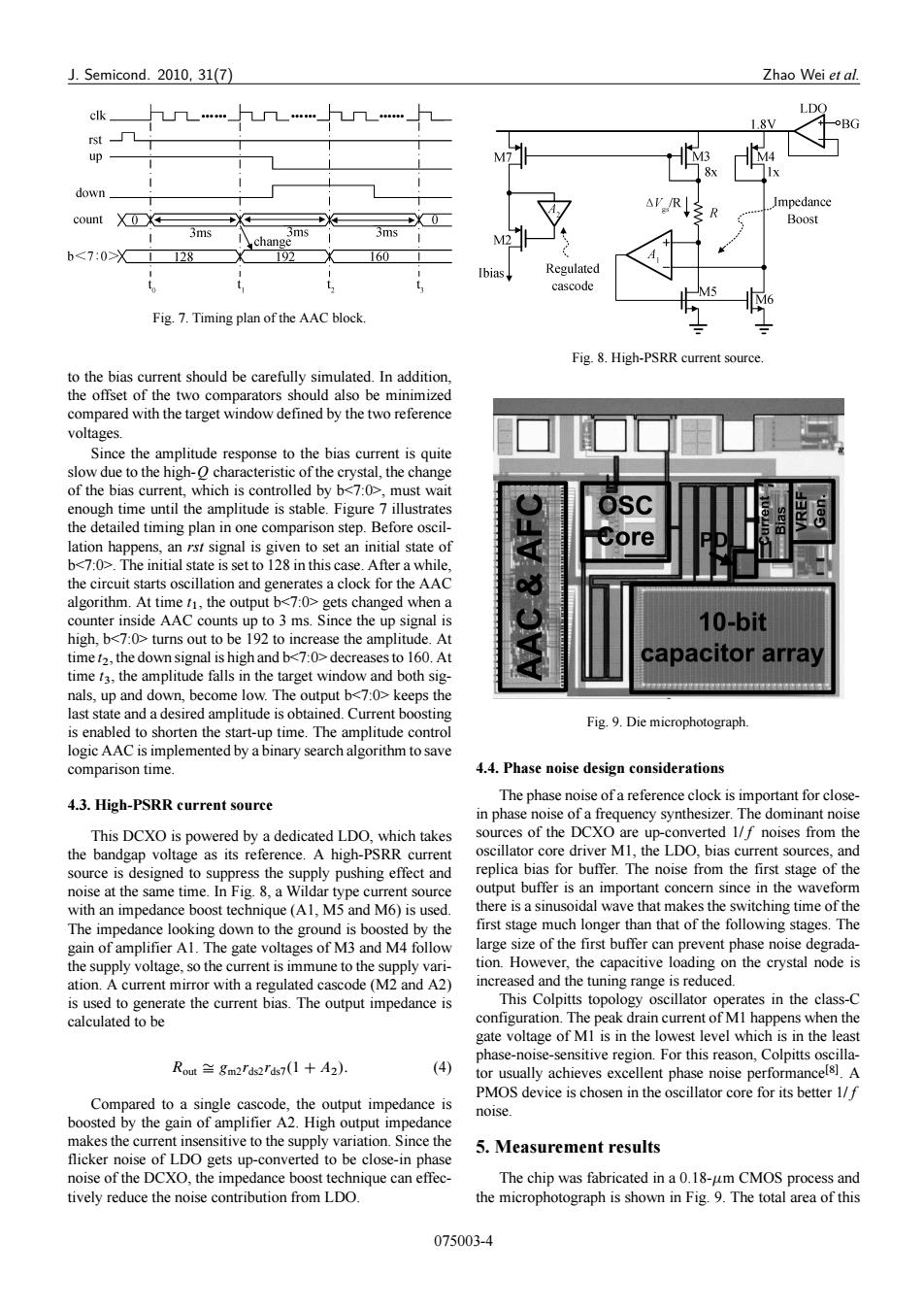
J.Semicond.2010,31(7) Zhao Wei et al. LDO clk_ 18V rst p M7 down △VR Impedance 3 R count Boost 3ms 3ms M2 b<7:0>X1128 192■ 160 Ibias Regulated to cascode Fig.7.Timing plan of the AAC block. Fig.8.High-PSRR current source. to the bias current should be carefully simulated.In addition. the offset of the two comparators should also be minimized compared with the target window defined by the two reference voltages. Since the amplitude response to the bias current is quite slow due to the high-O characteristic of the crystal,the change of the bias current,which is controlled by b<7:0>,must wait enough time until the amplitude is stable.Figure 7 illustrates the detailed timing plan in one comparison step.Before oscil- e lation happens,an rst signal is given to set an initial state of b<7:0>.The initial state is set to 128 in this case.After a while, the circuit starts oscillation and generates a clock for the AAC algorithm.At time n,the output b<7:0>gets changed when a counter inside AAC counts up to 3 ms.Since the up signal is 10-bit high.b<7:0>turns out to be 192 to increase the amplitude.At time t2,the down signal is high and b<7:0>decreases to 160.At capacitor array time t3,the amplitude falls in the target window and both sig- nals,up and down,become low.The output b<7:0>keeps the last state and a desired amplitude is obtained.Current boosting Fig.9.Die microphotograph is enabled to shorten the start-up time.The amplitude control logic AAC is implemented by a binary search algorithm to save comparison time. 4.4.Phase noise design considerations The phase noise of a reference clock is important for close- 4.3.High-PSRR current source in phase noise of a frequency synthesizer.The dominant noise This DCXO is powered by a dedicated LDO,which takes sources of the DCXO are up-converted 1/f noises from the the bandgap voltage as its reference.A high-PSRR current oscillator core driver M1,the LDO,bias current sources,and source is designed to suppress the supply pushing effect and replica bias for buffer.The noise from the first stage of the noise at the same time.In Fig.8,a Wildar type current source output buffer is an important concern since in the waveform with an impedance boost technique(Al,M5 and M6)is used. there is a sinusoidal wave that makes the switching time of the The impedance looking down to the ground is boosted by the first stage much longer than that of the following stages.The gain of amplifier Al.The gate voltages of M3 and M4 follow large size of the first buffer can prevent phase noise degrada- the supply voltage,so the current is immune to the supply vari- tion.However,the capacitive loading on the crystal node is ation.A current mirror with a regulated cascode(M2 and A2) increased and the tuning range is reduced. is used to generate the current bias.The output impedance is This Colpitts topology oscillator operates in the class-C calculated to be configuration.The peak drain current of MI happens when the gate voltage of MI is in the lowest level which is in the least phase-noise-sensitive region.For this reason,Colpitts oscilla- Rout gm2rds2rds7(1 +A2). (4) tor usually achieves excellent phase noise performancel81.A PMOS device is chosen in the oscillator core for its better 1/f Compared to a single cascode,the output impedance is noise. boosted by the gain of amplifier A2.High output impedance makes the current insensitive to the supply variation.Since the 5.Measurement results flicker noise of LDO gets up-converted to be close-in phase noise of the DCXO,the impedance boost technique can effec- The chip was fabricated in a 0.18-um CMOS process and tively reduce the noise contribution from LDO. the microphotograph is shown in Fig.9.The total area of this 075003-4J. Semicond. 2010, 31(7) Zhao Wei et al. Fig. 7. Timing plan of the AAC block. to the bias current should be carefully simulated. In addition, the offset of the two comparators should also be minimized compared with the target window defined by the two reference voltages. Since the amplitude response to the bias current is quite slow due to the high-Q characteristic of the crystal, the change of the bias current, which is controlled by b<7:0>, must wait enough time until the amplitude is stable. Figure 7 illustrates the detailed timing plan in one comparison step. Before oscillation happens, an rst signal is given to set an initial state of b<7:0>. The initial state is set to 128 in this case. After a while, the circuit starts oscillation and generates a clock for the AAC algorithm. At time t1, the output b<7:0> gets changed when a counter inside AAC counts up to 3 ms. Since the up signal is high, b<7:0> turns out to be 192 to increase the amplitude. At time t2, the down signal is high and b<7:0> decreases to 160. At time t3, the amplitude falls in the target window and both signals, up and down, become low. The output b<7:0> keeps the last state and a desired amplitude is obtained. Current boosting is enabled to shorten the start-up time. The amplitude control logic AAC is implemented by a binary search algorithm to save comparison time. 4.3. High-PSRR current source This DCXO is powered by a dedicated LDO, which takes the bandgap voltage as its reference. A high-PSRR current source is designed to suppress the supply pushing effect and noise at the same time. In Fig. 8, a Wildar type current source with an impedance boost technique (A1, M5 and M6) is used. The impedance looking down to the ground is boosted by the gain of amplifier A1. The gate voltages of M3 and M4 follow the supply voltage, so the current is immune to the supply variation. A current mirror with a regulated cascode (M2 and A2) is used to generate the current bias. The output impedance is calculated to be Rout Š gm2rds2rds7.1 C A2/: (4) Compared to a single cascode, the output impedance is boosted by the gain of amplifier A2. High output impedance makes the current insensitive to the supply variation. Since the flicker noise of LDO gets up-converted to be close-in phase noise of the DCXO, the impedance boost technique can effectively reduce the noise contribution from LDO. Fig. 8. High-PSRR current source. Fig. 9. Die microphotograph. 4.4. Phase noise design considerations The phase noise of a reference clock is important for closein phase noise of a frequency synthesizer. The dominant noise sources of the DCXO are up-converted 1/f noises from the oscillator core driver M1, the LDO, bias current sources, and replica bias for buffer. The noise from the first stage of the output buffer is an important concern since in the waveform there is a sinusoidal wave that makes the switching time of the first stage much longer than that of the following stages. The large size of the first buffer can prevent phase noise degradation. However, the capacitive loading on the crystal node is increased and the tuning range is reduced. This Colpitts topology oscillator operates in the class-C configuration. The peak drain current of M1 happens when the gate voltage of M1 is in the lowest level which is in the least phase-noise-sensitive region. For this reason, Colpitts oscillator usually achieves excellent phase noise performanceŒ8. A PMOS device is chosen in the oscillator core for its better 1/f noise. 5. Measurement results The chip was fabricated in a 0.18-m CMOS process and the microphotograph is shown in Fig. 9. The total area of this 075003-4