正在加载图片...
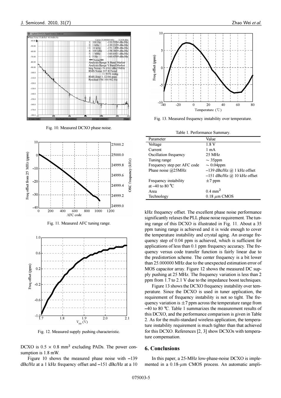
J.Semicond.2010,31(7) Zhao Wei et al. 10ch kef-4 0 10 -110 RM 1040 -20 0 20 40 60 80 Temperature (C) 12. Fig.13.Measured frequency instability over temperature Fig.10.Measured DCXO phase noise. Table 1.Performance Summary. Parameter Value 25000.2 Voltage 1.8V Current I mA 250000 Oscillation frequency 25 MHz Tuning range 35ppm 24999.8 Frequency step per AFC code ~0.04ppm -10 Phase noise @25MHz -139 dBc/Hz 1 kHz offset 24999.6 -151 dBc/Hz 10 kHz offset -20 Frequency instability 土7ppm 24999.4 at-40to80℃ 30 Area 0.4mm2 24999.2 Technology 0.18 um CMOS 24999.0 200 400600800 10001200 AFC code kHz frequency offset.The excellent phase noise performance significantly relaxes the PLL phase noise requirement.The tun- Fig.11.Measured AFC tuning range. ing range of this DCXO is illustrated in Fig.11.About a 35 ppm tuning range is achieved and it is wide enough to cover the temperature instability and crystal aging.An average fre- 1.0 quency step of 0.04 ppm is achieved,which is sufficient for applications of less than 0.1 ppm frequency accuracy.The fre- 0.6 quency versus code transfer function is fairly linear due to the predistortion scheme.The center frequency is a bit lower than 25.000000 MHz due to the unexpected estimation error of 0.2 MOS capacitor array.Figure 12 shows the measured DC sup- ply pushing at 25 MHz.The frequency variation is less than 2 ppm from 1.7 to 2.1 V due to the impedance boost techniques. -0.2 Figure 13 shows the DCXO frequency instability over tem- perature.Since the DCXO is used in tuner application,the requirement of frequency instability is not so tight.The fre- -0.6 quency variation is+7 ppm across the temperature range from -40 to 80 C.Table 1 summarizes the measurement results of 1 this DCXO,and the performance comparison is given in Table 1.8 1.9 2.0 V(V) 2.As for the multi-standard wireless application,the tempera- ture instability requirement is much tighter than that achieved Fig.12.Measured supply pushing characteristic for this DCXO.References [2,3]show DCXOs with tempera- ture compensation. DCXO is 0.5 x 0.8 mm2 excluding PADs.The power con- 6.Conclusions sumption is 1.8 mW. Figure 10 shows the measured phase noise with-139 In this paper,a 25-MHz low-phase-noise DCXO is imple- dBc/Hz at a I kHz frequency offset and-151 dBc/Hz at a 10 mented in a 0.18-um CMOS process.An automatic ampli- 075003-5J. Semicond. 2010, 31(7) Zhao Wei et al. Fig. 10. Measured DCXO phase noise. Fig. 11. Measured AFC tuning range. Fig. 12. Measured supply pushing characteristic. DCXO is 0.5 0.8 mm2 excluding PADs. The power consumption is 1.8 mW. Figure 10 shows the measured phase noise with –139 dBc/Hz at a 1 kHz frequency offset and –151 dBc/Hz at a 10 Fig. 13. Measured frequency instability over temperature. Table 1. Performance Summary. Parameter Value Voltage 1.8 V Current 1 mA Oscillation frequency 25 MHz Tuning range 35ppm Frequency step per AFC code 0:04ppm Phase noise @25MHz –139 dBc/Hz @ 1 kHz offset –151 dBc/Hz @ 10 kHz offset Frequency instability at –40 to 80 ıC ˙7 ppm Area 0.4 mm2 Technology 0.18 m CMOS kHz frequency offset. The excellent phase noise performance significantly relaxes the PLL phase noise requirement. The tuning range of this DCXO is illustrated in Fig. 11. About a 35 ppm tuning range is achieved and it is wide enough to cover the temperature instability and crystal aging. An average frequency step of 0.04 ppm is achieved, which is sufficient for applications of less than 0.1 ppm frequency accuracy. The frequency versus code transfer function is fairly linear due to the predistortion scheme. The center frequency is a bit lower than 25.000000 MHz due to the unexpected estimation error of MOS capacitor array. Figure 12 shows the measured DC supply pushing at 25 MHz. The frequency variation is less than 2 ppm from 1.7 to 2.1 V due to the impedance boost techniques. Figure 13 shows the DCXO frequency instability over temperature. Since the DCXO is used in tuner application, the requirement of frequency instability is not so tight. The frequency variation is ˙7 ppm across the temperature range from –40 to 80 ıC. Table 1 summarizes the measurement results of this DCXO, and the performance comparison is given in Table 2. As for the multi-standard wireless application, the temperature instability requirement is much tighter than that achieved for this DCXO. References [2, 3] show DCXOs with temperature compensation. 6. Conclusions In this paper, a 25-MHz low-phase-noise DCXO is implemented in a 0.18-m CMOS process. An automatic ampli- 075003-5�