正在加载图片...

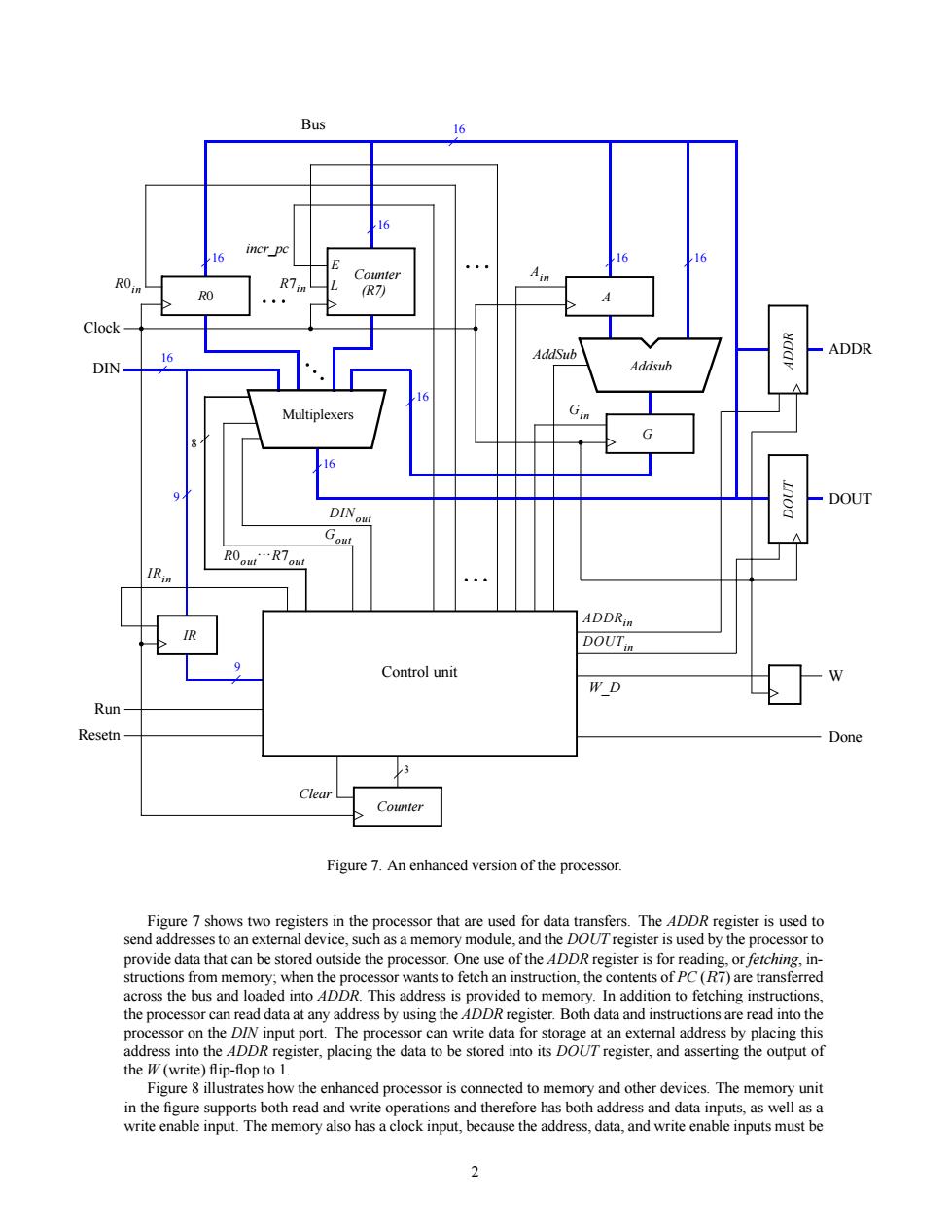
Bus DOUT ADDR. Control unit Resetr Clear Figure 7.An enhanced version of the processor. Figure 7 shows two registers in the processor that are used for data transfers.The 4DDR register is used to send addresses to an external device,such as a memory module,and the DOUTregister is used by the processor to provide data that can be stored eus the processor can read data at any address by using the ADDR register.Both data and instructions are read into the in-op Figure 8 illustrates how the enhanced processor is connected to memory and other devices.The memory unit in the figure supports both read and write operations and therefore has both address and data inputs,as well as a write enable input.The memory also has a clock input,because the address,data,and write enable inputs must beControl unit AddSub Ain Gin Run Done 9 16 16 DIN R0in Multiplexers R7in Bus Clock Gout R0out}R7out 16 R0 Counter 16 8 DINout 16 IRin Addsub 16 IR 9 A G ADDR Counter DOUT ADDRin ADDR DOUT W W_D 3 Clear Resetn (R7) L E incr_pc DOUTin 16 16 Figure 7. An enhanced version of the processor. Figure 7 shows two registers in the processor that are used for data transfers. The ADDR register is used to send addresses to an external device, such as a memory module, and the DOUT register is used by the processor to provide data that can be stored outside the processor. One use of the ADDR register is for reading, or fetching, instructions from memory; when the processor wants to fetch an instruction, the contents of PC (R7) are transferred across the bus and loaded into ADDR. This address is provided to memory. In addition to fetching instructions, the processor can read data at any address by using the ADDR register. Both data and instructions are read into the processor on the DIN input port. The processor can write data for storage at an external address by placing this address into the ADDR register, placing the data to be stored into its DOUT register, and asserting the output of the W (write) flip-flop to 1. Figure 8 illustrates how the enhanced processor is connected to memory and other devices. The memory unit in the figure supports both read and write operations and therefore has both address and data inputs, as well as a write enable input. The memory also has a clock input, because the address, data, and write enable inputs must be 2