正在加载图片...
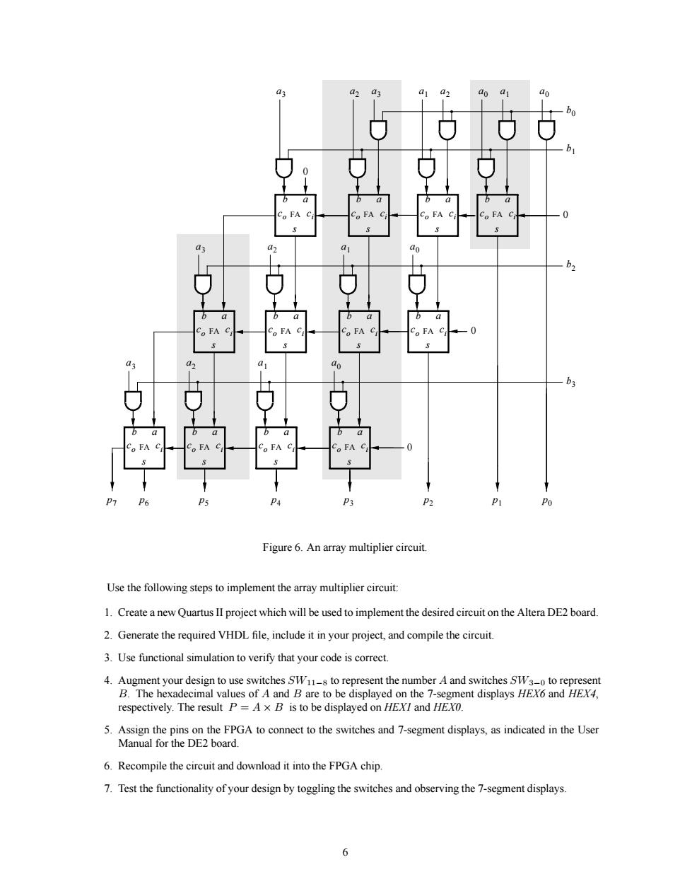
i6i666 但 的的的这 的的 Figure 6.An array multiplier circuit. Use the following steps to implement the array multiplier circuit 1.Create anew Quartus II project which will be used toimplement the desired circuit on the Altera DE2 board. 2.Generate the required VHDLfile,include it n your project,and compile the circui 3.Use functional simulation to verify that your code is correct 4.Au respectively.The result P=Ax B is to be displayed on HEXI and HEX0. 5.Assign the pins on the FPGA to connect to the switches and 7-segment displays,as indicated in the User Manual for the DE2 board. 6.Recompile the circuit and download it into the FPGA chip. 7.Test the functionality of your design by toggling the switches and observing the 7-segment displays. 6a1 FA ci b a co s FA ci b a co s a2 a3 b0 b1 b2 a0 FA ci b a co s b3 a0 FA ci b a co s FA ci b a co s a1 a2 0 FA ci b a co s a0 a1 0 0 a0 a2 FA ci b a co s FA ci b a co s a3 a1 FA ci b a co s 0 a3 FA ci b a co s a2 FA ci b a co s a3 FA ci b a co s p0 p1 p2 p3 p4 p6 p7 p5 Figure 6. An array multiplier circuit. Use the following steps to implement the array multiplier circuit: 1. Create a new Quartus II project which will be used to implement the desired circuit on the Altera DE2 board. 2. Generate the required VHDL file, include it in your project, and compile the circuit. 3. Use functional simulation to verify that your code is correct. 4. Augment your design to use switches SW11−8 to represent the number A and switches SW3−0 to represent B. The hexadecimal values of A and B are to be displayed on the 7-segment displays HEX6 and HEX4, respectively. The result P = A × B is to be displayed on HEX1 and HEX0. 5. Assign the pins on the FPGA to connect to the switches and 7-segment displays, as indicated in the User Manual for the DE2 board. 6. Recompile the circuit and download it into the FPGA chip. 7. Test the functionality of your design by toggling the switches and observing the 7-segment displays. 6