正在加载图片...
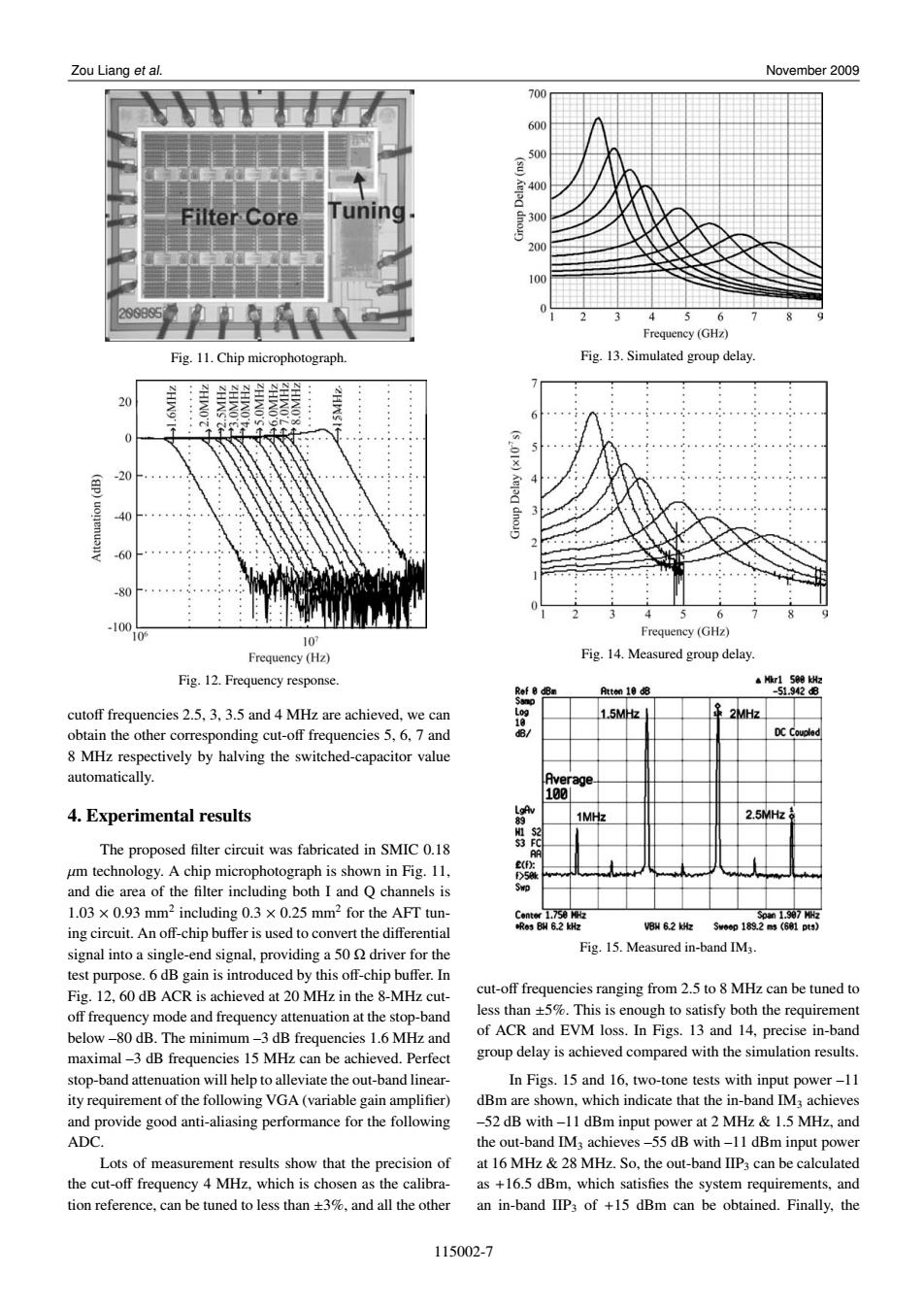
Zou Liang et al. November 2009 700 600 400 uning- (su)dno 300 200 100 456 Frequency(GHz) Fig.11.Chip microphotograph Fig.13.Simulated group delay 30 s -20 40 201x)Kelad dnouD -60 -80 4 5 -100 0 Frequency(GHz) 10 Frequency (Hz) Fig.14.Measured group delay Fig.12.Frequency response. Mkr1 508 kH: Rof Atten 10 dB -51.9428 cutoff frequencies 2.5,3,3.5 and 4 MHz are achieved,we can 15MH也 2MHz obtain the other corresponding cut-off frequencies 5.6.7 and 8 MHz respectively by halving the switched-capacitor value automatically Average 100 4.Experimental results 1MHz 2.5MHz The proposed filter circuit was fabricated in SMIC 0.18 um technology.A chip microphotograph is shown in Fig.11, and die area of the filter including both I and Q channels is Swp 1.03 x 0.93 mm2 including 0.3 x 0.25 mm2 for the AFT tun- Center 1.750 MHz S01.907HHE ing circuit.An off-chip buffer is used to convert the differential R5B刚62k州 VBm62地 S#66p189.2ms(601pts) signal into a single-end signal,providing a 50 driver for the Fig.15.Measured in-band IM3. test purpose.6 dB gain is introduced by this off-chip buffer.In Fig.12.60 dB ACR is achieved at 20 MHz in the 8-MHz cut- cut-off frequencies ranging from 2.5 to 8 MHz can be tuned to off frequency mode and frequency attenuation at the stop-band less than +5%.This is enough to satisfy both the requirement below-80 dB.The minimum-3 dB frequencies 1.6 MHz and of ACR and EVM loss.In Figs.13 and 14,precise in-band maximal-3 dB frequencies 15 MHz can be achieved.Perfect group delay is achieved compared with the simulation results. stop-band attenuation will help to alleviate the out-band linear- In Figs.15 and 16,two-tone tests with input power-11 ity requirement of the following VGA(variable gain amplifier) dBm are shown.which indicate that the in-band IM achieves and provide good anti-aliasing performance for the following -52 dB with-11 dBm input power at 2 MHz 1.5 MHz,and ADC. the out-band IM3 achieves-55 dB with-11 dBm input power Lots of measurement results show that the precision of at 16 MHz 28 MHz.So,the out-band IIP3 can be calculated the cut-off frequency 4 MHz,which is chosen as the calibra- as +16.5 dBm,which satisfies the system requirements,and tion reference,can be tuned to less than +3%,and all the other an in-band IIP3 of +15 dBm can be obtained.Finally,the 115002-7Zou Liang et al. November 2009 Fig. 11. Chip microphotograph. Fig. 12. Frequency response. cutoff frequencies 2.5, 3, 3.5 and 4 MHz are achieved, we can obtain the other corresponding cut-off frequencies 5, 6, 7 and 8 MHz respectively by halving the switched-capacitor value automatically. 4. Experimental results The proposed filter circuit was fabricated in SMIC 0.18 µm technology. A chip microphotograph is shown in Fig. 11, and die area of the filter including both I and Q channels is 1.03 × 0.93 mm2 including 0.3 × 0.25 mm2 for the AFT tuning circuit. An off-chip buffer is used to convert the differential signal into a single-end signal, providing a 50 Ω driver for the test purpose. 6 dB gain is introduced by this off-chip buffer. In Fig. 12, 60 dB ACR is achieved at 20 MHz in the 8-MHz cutoff frequency mode and frequency attenuation at the stop-band below –80 dB. The minimum –3 dB frequencies 1.6 MHz and maximal –3 dB frequencies 15 MHz can be achieved. Perfect stop-band attenuation will help to alleviate the out-band linearity requirement of the following VGA (variable gain amplifier) and provide good anti-aliasing performance for the following ADC. Lots of measurement results show that the precision of the cut-off frequency 4 MHz, which is chosen as the calibration reference, can be tuned to less than ±3%, and all the other Fig. 13. Simulated group delay. Fig. 14. Measured group delay. Fig. 15. Measured in-band IM3. cut-off frequencies ranging from 2.5 to 8 MHz can be tuned to less than ±5%. This is enough to satisfy both the requirement of ACR and EVM loss. In Figs. 13 and 14, precise in-band group delay is achieved compared with the simulation results. In Figs. 15 and 16, two-tone tests with input power –11 dBm are shown, which indicate that the in-band IM3 achieves –52 dB with –11 dBm input power at 2 MHz & 1.5 MHz, and the out-band IM3 achieves –55 dB with –11 dBm input power at 16 MHz & 28 MHz. So, the out-band IIP3 can be calculated as +16.5 dBm, which satisfies the system requirements, and an in-band IIP3 of +15 dBm can be obtained. Finally, the 115002-7