正在加载图片...
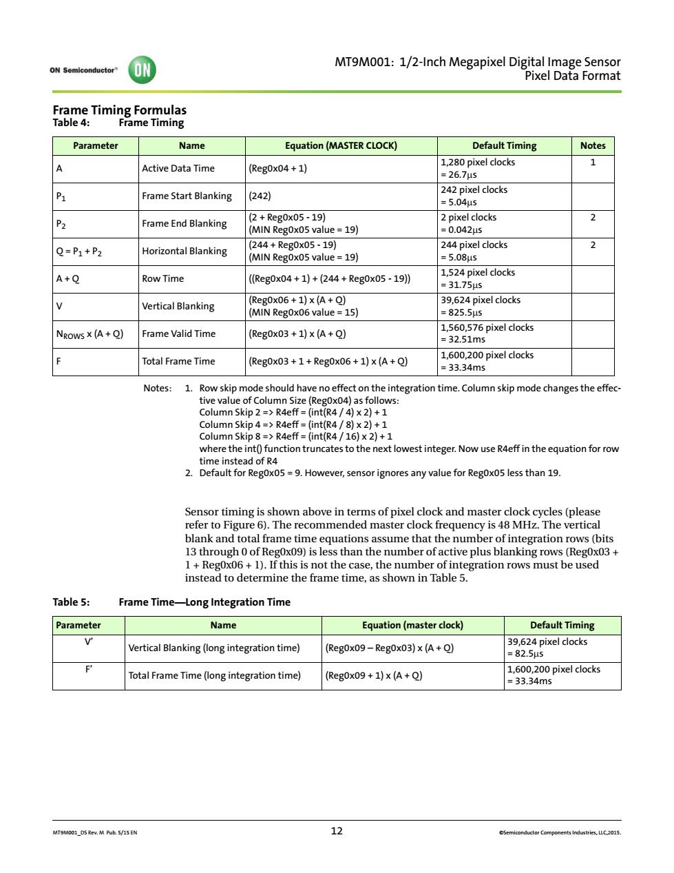
d M9wo1:1/2HnchMe8apeDealDaBeienmiat Timi Parameter Name Equation (MASTER CLOCK) Default Timing Notes A Active Data Time Reg0x04+1) 1 pixel clocks 1 Frame Start Blanking (242 5a8edoc P2 Frame End Blanking 2+Reg0x05-19) 2 pixel clocks (MIN Regoxo5 value 19) =0.042μs Q-P1+P2 Horizontal Blanking (244+Reg0x05-19) 244 pixel clocks 2 (MIN Regoxo5 value-19) A+Q Row Time (Reg0x04+1)+(244+Reg0x05-19 Vertical Blanking Ngows x(A+Q)Frame Valid Time (Reg0x03+1)X(A+Q】 1,560,576 pixel clocks 3 Total Frame Time (Reg0x03+1+Regox06+1)x (A+Q) Notes:1.Row skip mode should have no effect on the integration time.Column skip mode changes the effec tive value Column Skip4=>R4eff=(int(R4/8)x2)+1 Column Skip 8 (int(R tiont es to)+ lowest integer.Now use R4eff in theequation for row 2 for=9.However,sensor ignores any value for RegoxO5 less than 19 Sensor timing is shown above in terms of pixel clock and master clock cycles(please Figure6 The recommended master cl ck frequency is 48 MHz.The vertica 13a 1+Regox06+D).If this is not the case.the number of integration rows must be used instead to determine the frame time,as shown in Table 5. Table5: Frame Time-Long Integration Time Parameter Name Equation(master dock) Default Timing Vertical Blanking(ng integration time) [RegOx09-RegOx03)x (A+Q) Total Frame Time(long integration time) (Reg0x09+1)×(a+Q) MTMO01 DS ReM Pub.S/I5 EN 名 MT9M001_DS Rev. M Pub. 5/15 EN 12 ©Semiconductor Components Industries, LLC,2015. MT9M001: 1/2-Inch Megapixel Digital Image Sensor Pixel Data Format Frame Timing Formulas Notes: 1. Row skip mode should have no effect on the integration time. Column skip mode changes the effective value of Column Size (Reg0x04) as follows: Column Skip 2 => R4eff = (int(R4 / 4) x 2) + 1 Column Skip 4 => R4eff = (int(R4 / 8) x 2) + 1 Column Skip 8 => R4eff = (int(R4 / 16) x 2) + 1 where the int() function truncates to the next lowest integer. Now use R4eff in the equation for row time instead of R4 2. Default for Reg0x05 = 9. However, sensor ignores any value for Reg0x05 less than 19. Sensor timing is shown above in terms of pixel clock and master clock cycles (please refer to Figure 6). The recommended master clock frequency is 48 MHz. The vertical blank and total frame time equations assume that the number of integration rows (bits 13 through 0 of Reg0x09) is less than the number of active plus blanking rows (Reg0x03 + 1 + Reg0x06 + 1). If this is not the case, the number of integration rows must be used instead to determine the frame time, as shown in Table 5. Table 4: Frame Timing Parameter Name Equation (MASTER CLOCK) Default Timing Notes A Active Data Time (Reg0x04 + 1) 1,280 pixel clocks = 26.7s 1 P1 Frame Start Blanking (242) 242 pixel clocks = 5.04s P2 Frame End Blanking (2 + Reg0x05 - 19) (MIN Reg0x05 value = 19) 2 pixel clocks = 0.042s 2 Q = P1 + P2 Horizontal Blanking (244 + Reg0x05 - 19) (MIN Reg0x05 value = 19) 244 pixel clocks = 5.08s 2 A + Q Row Time ((Reg0x04 + 1) + (244 + Reg0x05 - 19)) 1,524 pixel clocks = 31.75s V Vertical Blanking (Reg0x06 + 1) x (A + Q) (MIN Reg0x06 value = 15) 39,624 pixel clocks = 825.5s NROWS x (A + Q) Frame Valid Time (Reg0x03 + 1) x (A + Q) 1,560,576 pixel clocks = 32.51ms F Total Frame Time (Reg0x03 + 1 + Reg0x06 + 1) x (A + Q) 1,600,200 pixel clocks = 33.34ms Table 5: Frame Time—Long Integration Time Parameter Name Equation (master clock) Default Timing V’ Vertical Blanking (long integration time) (Reg0x09 – Reg0x03) x (A + Q) 39,624 pixel clocks = 82.5s F’ Total Frame Time (long integration time) (Reg0x09 + 1) x (A + Q) 1,600,200 pixel clocks = 33.34ms