正在加载图片...
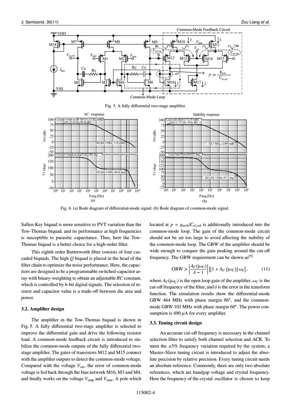
J.Semicond.30(11) Zou Liang et al. Common-Mode Feedback Circuit VDD M13 Re Ce Common-Mode Loop Fig.5.A fully differential two-stage amplifier. AC response Stability response 100 100C 75 (p)OA 155023 ()O 50 25 02300 25 150 125 1 75 2I02.7.59.72cd) 10 10 1010101010心10101010 10101 10炉10101051010710心10 Freq (Hz) Freq (Hz) (a) (b) Fig.6.(a)Bode diagram of differential-mode signal;(b)Bode diagram of common-mode signal Sallen-Key biquad is more sensitive to PVT variation than the located at p =gmi6/Cnito is additionally introduced into the Tow-Thomas biquad,and its performance at high frequencies common-mode loop.The gain of the common-mode circuit is susceptible to parasitic capacitance.Thus,here the Tow- should not be set too large to avoid affecting the stability of Thomas biquad is a better choice for a high-order filter. the common-mode loop.The GBW of the amplifier should be This eighth order Butterworth filter consists of four cas wide enough to conquer the gain peaking around the cut-off caded biquads.The high O biquad is placed in the head of the frequency.The GBW requirement can be shown as[51 filter chain to optimize the noise performance.Here,the capac- itors are designed to be a programmable switched-capacitor ar- GBW≥ geelL+ac0aeoaue. (11) ray with binary-weighting to obtain an adjustable RC constant, where Ac(j@c)is the open loop gain of the amplifier,wc is the which is controlled by 6-bit digital signals.The selection of re- cut-off frequency of the filter,and 6 is the error in the transform sistor and capacitor value is a trade-off between die area and function.The simulation results show the differential-mode power. GBW 464 MHz with phase margin 86,and the common- 3.2.Amplifier design mode GBW 103 MHz with phase margin 60.The power con- sumption is 490 uA for every amplifier. The amplifier in the Tow-Thomas biquad is shown in 3.3.Tuning circuit design Fig.5.A fully differential two-stage amplifier is selected to improve the differential gain and drive the following resistor An accurate cut-off frequency is necessary in the channel load.A common-mode feedback circuit is introduced to sta- selection filter to satisfy both channel selection and ACR.To bilize the common-mode outputs of the fully differential two- meet the +5%frequency variation required by the system,a stage amplifier.The gates of transistors M12 and M15 connect Master-Slave tuning circuit is introduced to adjust the abso- with the amplifier outputs to detect the common-mode voltage. lute precision by relative precision.Every tuning circuit needs Compared with the voltage Vem,the error of common-mode an absolute reference.Commonly,there are only two absolute voltage is fed back through the bias network M16.M3 and M4. references,which are bandgap voltage and crystal frequency and finally works on the voltage Voutp and Voutn.A pole which Here the frequency of the crystal oscillator is chosen to keep 115002-4J. Semicond. 30(11) Zou Liang et al. Fig. 5. A fully differential two-stage amplifier. Fig. 6. (a) Bode diagram of differential-mode signal; (b) Bode diagram of common-mode signal. Sallen-Key biquad is more sensitive to PVT variation than the Tow-Thomas biquad, and its performance at high frequencies is susceptible to parasitic capacitance. Thus, here the TowThomas biquad is a better choice for a high-order filter. This eighth order Butterworth filter consists of four cascaded biquads. The high Q biquad is placed in the head of the filter chain to optimize the noise performance. Here, the capacitors are designed to be a programmable switched-capacitor array with binary-weighting to obtain an adjustable RC constant, which is controlled by 6-bit digital signals. The selection of resistor and capacitor value is a trade-off between die area and power. 3.2. Amplifier design The amplifier in the Tow-Thomas biquad is shown in Fig. 5. A fully differential two-stage amplifier is selected to improve the differential gain and drive the following resistor load. A common-mode feedback circuit is introduced to stabilize the common-mode outputs of the fully differential twostage amplifier. The gates of transistors M12 and M15 connect with the amplifier outputs to detect the common-mode voltage. Compared with the voltage Vcm, the error of common-mode voltage is fed back through the bias network M16, M3 and M4, and finally works on the voltage Voutp and Voutn. A pole which located at p = gm16/Cn1,tol is additionally introduced into the common-mode loop. The gain of the common-mode circuit should not be set too large to avoid affecting the stability of the common-mode loop. The GBW of the amplifier should be wide enough to conquer the gain peaking around the cut-off frequency. The GBW requirement can be shown as[5] GBW >
AC(jωC) δ − 1
[ 1 + AC ( jωC )]ωC
, (11) where AC(jωC ) is the open loop gain of the amplifier, ωC is the cut-off frequency of the filter, and δ is the error in the transform function. The simulation results show the differential-mode GBW 464 MHz with phase margin 86◦ , and the commonmode GBW 103 MHz with phase margin 60◦ . The power consumption is 490 µA for every amplifier. 3.3. Tuning circuit design An accurate cut-off frequency is necessary in the channel selection filter to satisfy both channel selection and ACR. To meet the ±5% frequency variation required by the system, a Master–Slave tuning circuit is introduced to adjust the absolute precision by relative precision. Every tuning circuit needs an absolute reference. Commonly, there are only two absolute references, which are bandgap voltage and crystal frequency. Here the frequency of the crystal oscillator is chosen to keep 115002-4