正在加载图片...
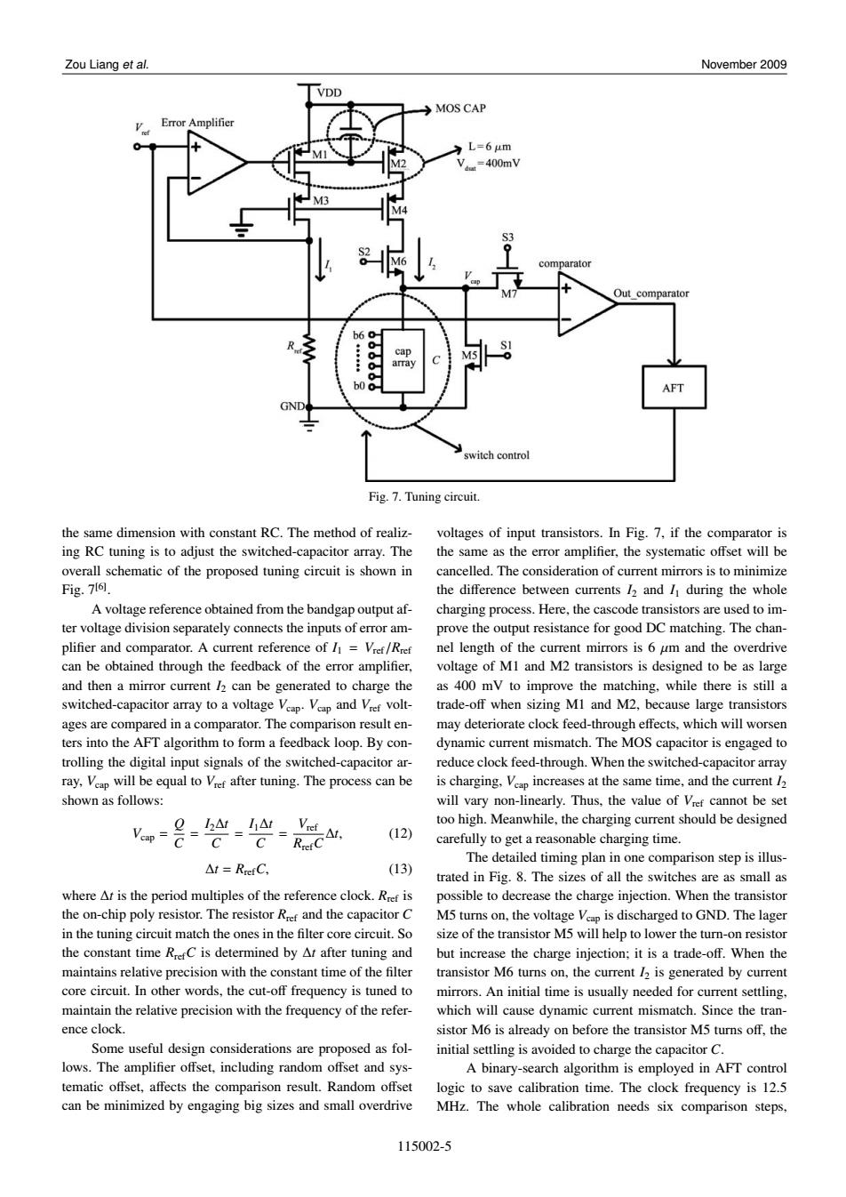
Zou Liang et al. November 2009 VDD MOS CAP Error Amplifier L=6 um =400mV S3 comparator Out comparator b6 o- 0 cap AFT GND switch control Fig.7.Tuning circuit. the same dimension with constant RC.The method of realiz- voltages of input transistors.In Fig.7,if the comparator is ing RC tuning is to adjust the switched-capacitor array.The the same as the error amplifier,the systematic offset will be overall schematic of the proposed tuning circuit is shown in cancelled.The consideration of current mirrors is to minimize Fig.7161. the difference between currents 12 and I during the whole A voltage reference obtained from the bandgap output af- charging process.Here,the cascode transistors are used to im- ter voltage division separately connects the inputs of error am- prove the output resistance for good DC matching.The chan- plifier and comparator.A current reference of /Vref/Rref nel length of the current mirrors is 6 um and the overdrive can be obtained through the feedback of the error amplifier, voltage of MI and M2 transistors is designed to be as large and then a mirror current /2 can be generated to charge the as 400 mV to improve the matching,while there is still a switched-capacitor array to a voltage Vap.Vap and Vef volt- trade-off when sizing MI and M2,because large transistors ages are compared in a comparator.The comparison result en- may deteriorate clock feed-through effects,which will worsen ters into the AFT algorithm to form a feedback loop.By con- dynamic current mismatch.The MOS capacitor is engaged to trolling the digital input signals of the switched-capacitor ar- reduce clock feed-through.When the switched-capacitor array ray,Veap will be equal to Vref after tuning.The process can be is charging.Veap increases at the same time,and the current 12 shown as follows: will vary non-linearly.Thus,the value of Vref cannot be set m=是-袋-g如 too high.Meanwhile,the charging current should be designed (12) carefully to get a reasonable charging time. The detailed timing plan in one comparison step is illus- △t=RefC, (13) trated in Fig.8.The sizes of all the switches are as small as where At is the period multiples of the reference clock.Rref is possible to decrease the charge injection.When the transistor the on-chip poly resistor.The resistor Rref and the capacitor C M5 turns on,the voltage Veap is discharged to GND.The lager in the tuning circuit match the ones in the filter core circuit.So size of the transistor M5 will help to lower the turn-on resistor the constant time RrerC is determined by At after tuning and but increase the charge injection:it is a trade-off.When the maintains relative precision with the constant time of the filter transistor M6 turns on,the current /2 is generated by current core circuit.In other words,the cut-off frequency is tuned to mirrors.An initial time is usually needed for current settling. maintain the relative precision with the frequency of the refer- which will cause dynamic current mismatch.Since the tran- ence clock. sistor M6 is already on before the transistor M5 turns off,the Some useful design considerations are proposed as fol- initial settling is avoided to charge the capacitor C. lows.The amplifier offset,including random offset and sys- A binary-search algorithm is employed in AFT control tematic offset,affects the comparison result.Random offset logic to save calibration time.The clock frequency is 12.5 can be minimized by engaging big sizes and small overdrive MHz.The whole calibration needs six comparison steps, 115002-5Zou Liang et al. November 2009 Fig. 7. Tuning circuit. the same dimension with constant RC. The method of realizing RC tuning is to adjust the switched-capacitor array. The overall schematic of the proposed tuning circuit is shown in Fig. 7[6] . A voltage reference obtained from the bandgap output after voltage division separately connects the inputs of error amplifier and comparator. A current reference of I1 = Vref/Rref can be obtained through the feedback of the error amplifier, and then a mirror current I2 can be generated to charge the switched-capacitor array to a voltage Vcap. Vcap and Vref voltages are compared in a comparator. The comparison result enters into the AFT algorithm to form a feedback loop. By controlling the digital input signals of the switched-capacitor array, Vcap will be equal to Vref after tuning. The process can be shown as follows: Vcap = Q C = I2∆t C = I1∆t C = Vref RrefC ∆t, (12) ∆t = RrefC, (13) where ∆t is the period multiples of the reference clock. Rref is the on-chip poly resistor. The resistor Rref and the capacitor C in the tuning circuit match the ones in the filter core circuit. So the constant time RrefC is determined by ∆t after tuning and maintains relative precision with the constant time of the filter core circuit. In other words, the cut-off frequency is tuned to maintain the relative precision with the frequency of the reference clock. Some useful design considerations are proposed as follows. The amplifier offset, including random offset and systematic offset, affects the comparison result. Random offset can be minimized by engaging big sizes and small overdrive voltages of input transistors. In Fig. 7, if the comparator is the same as the error amplifier, the systematic offset will be cancelled. The consideration of current mirrors is to minimize the difference between currents I2 and I1 during the whole charging process. Here, the cascode transistors are used to improve the output resistance for good DC matching. The channel length of the current mirrors is 6 µm and the overdrive voltage of M1 and M2 transistors is designed to be as large as 400 mV to improve the matching, while there is still a trade-off when sizing M1 and M2, because large transistors may deteriorate clock feed-through effects, which will worsen dynamic current mismatch. The MOS capacitor is engaged to reduce clock feed-through. When the switched-capacitor array is charging, Vcap increases at the same time, and the current I2 will vary non-linearly. Thus, the value of Vref cannot be set too high. Meanwhile, the charging current should be designed carefully to get a reasonable charging time. The detailed timing plan in one comparison step is illustrated in Fig. 8. The sizes of all the switches are as small as possible to decrease the charge injection. When the transistor M5 turns on, the voltage Vcap is discharged to GND. The lager size of the transistor M5 will help to lower the turn-on resistor but increase the charge injection; it is a trade-off. When the transistor M6 turns on, the current I2 is generated by current mirrors. An initial time is usually needed for current settling, which will cause dynamic current mismatch. Since the transistor M6 is already on before the transistor M5 turns off, the initial settling is avoided to charge the capacitor C. A binary-search algorithm is employed in AFT control logic to save calibration time. The clock frequency is 12.5 MHz. The whole calibration needs six comparison steps, 115002-5