正在加载图片...
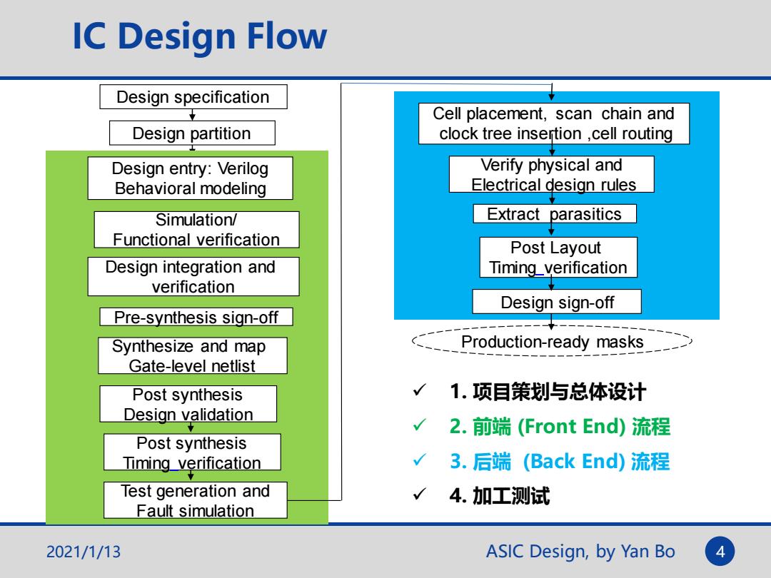
IC Design Flow Design specification Cell placement,scan chain and Design partition clock tree insertion cell routing Design entry:Verilog Verify physical and Behavioral modeling Electrical design rules Simulation/ Extract parasitics Functional verification Post Layout Design integration and Timing_verification verification Design sign-off Pre-synthesis sign-off Synthesize and map Production-ready masks Gate-level netlist Post synthesis 1.项目策划与总体设计 Design validation 2.前端(Front End)流程 Post synthesis Timing verification 3.后端(Back End)流程 Test generation and 4.加工测试 Fault simulation 2021/1/13 ASIC Design,by Yan BoASIC Design, by Yan Bo Cell placement, scan chain and clock tree insertion ,cell routing Verify physical and Electrical design rules Extract parasitics Design sign-off Production-ready masks IC Design Flow Design partition Design entry: Verilog Behavioral modeling Simulation/ Functional verification Design integration and verification Pre-synthesis sign-off Synthesize and map Gate-level netlist Post synthesis Design validation Post synthesis Timing verification Test generation and Fault simulation Design specification Post Layout Timing verification ✓ 1. 项目策划与总体设计 ✓ 2. 前端 (Front End) 流程 ✓ 3. 后端 (Back End) 流程 ✓ 4. 加工测试 2021/1/13 4