Topic2:FPGA Design with Verilog FPGA Design Method Design flow tools Deign Model of Verilog HDL Design style of Verilog HDL Design Examples 。RTL level design Components of Datapath Components of Controller Supplementary 。Synthesizable 。Some experiences 。Other syntax rules 2021/1/13 ASIC Design,by Yan Bo 3
ASIC Design, by Yan Bo Topic2: FPGA Design with Verilog FPGA Design Method Design flow & tools Deign Model of Verilog HDL Design style of Verilog HDL Design Examples • RTL level design • Components of Datapath • Components of Controller Supplementary • Synthesizable • Some experiences • Other syntax rules 2021/1/13 3
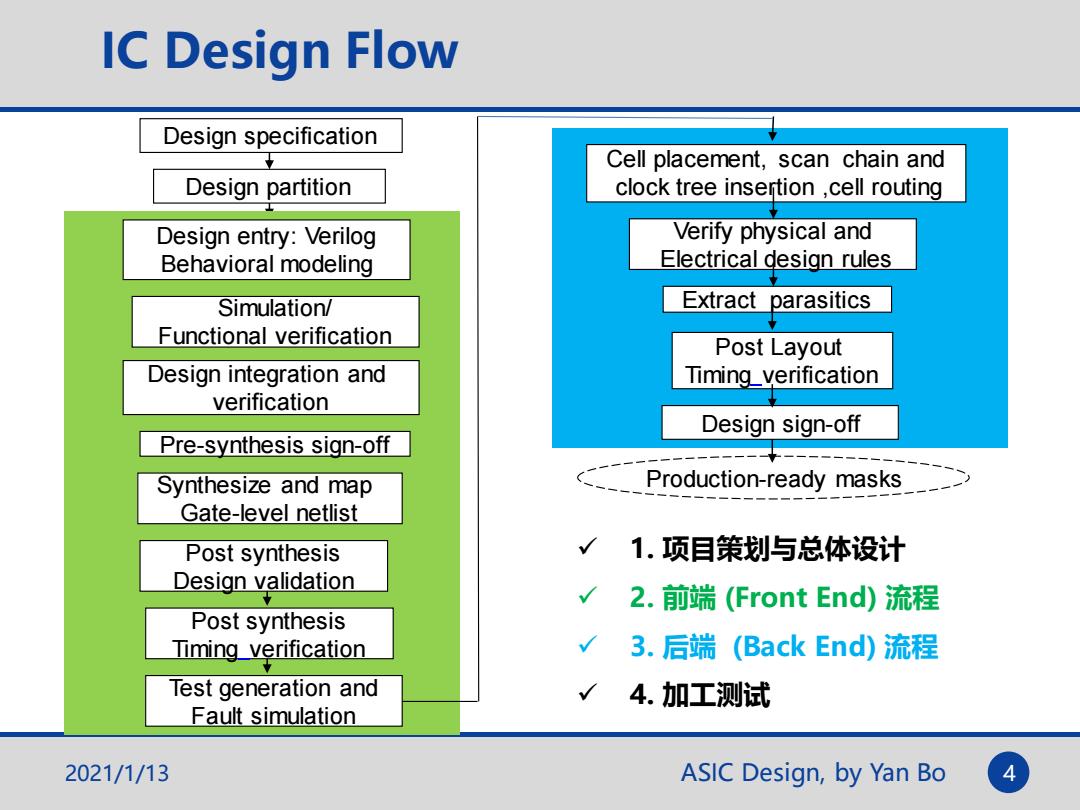
IC Design Flow Design specification Cell placement,scan chain and Design partition clock tree insertion cell routing Design entry:Verilog Verify physical and Behavioral modeling Electrical design rules Simulation/ Extract parasitics Functional verification Post Layout Design integration and Timing_verification verification Design sign-off Pre-synthesis sign-off Synthesize and map Production-ready masks Gate-level netlist Post synthesis 1.项目策划与总体设计 Design validation 2.前端(Front End)流程 Post synthesis Timing verification 3.后端(Back End)流程 Test generation and 4.加工测试 Fault simulation 2021/1/13 ASIC Design,by Yan Bo
ASIC Design, by Yan Bo Cell placement, scan chain and clock tree insertion ,cell routing Verify physical and Electrical design rules Extract parasitics Design sign-off Production-ready masks IC Design Flow Design partition Design entry: Verilog Behavioral modeling Simulation/ Functional verification Design integration and verification Pre-synthesis sign-off Synthesize and map Gate-level netlist Post synthesis Design validation Post synthesis Timing verification Test generation and Fault simulation Design specification Post Layout Timing verification ✓ 1. 项目策划与总体设计 ✓ 2. 前端 (Front End) 流程 ✓ 3. 后端 (Back End) 流程 ✓ 4. 加工测试 2021/1/13 4
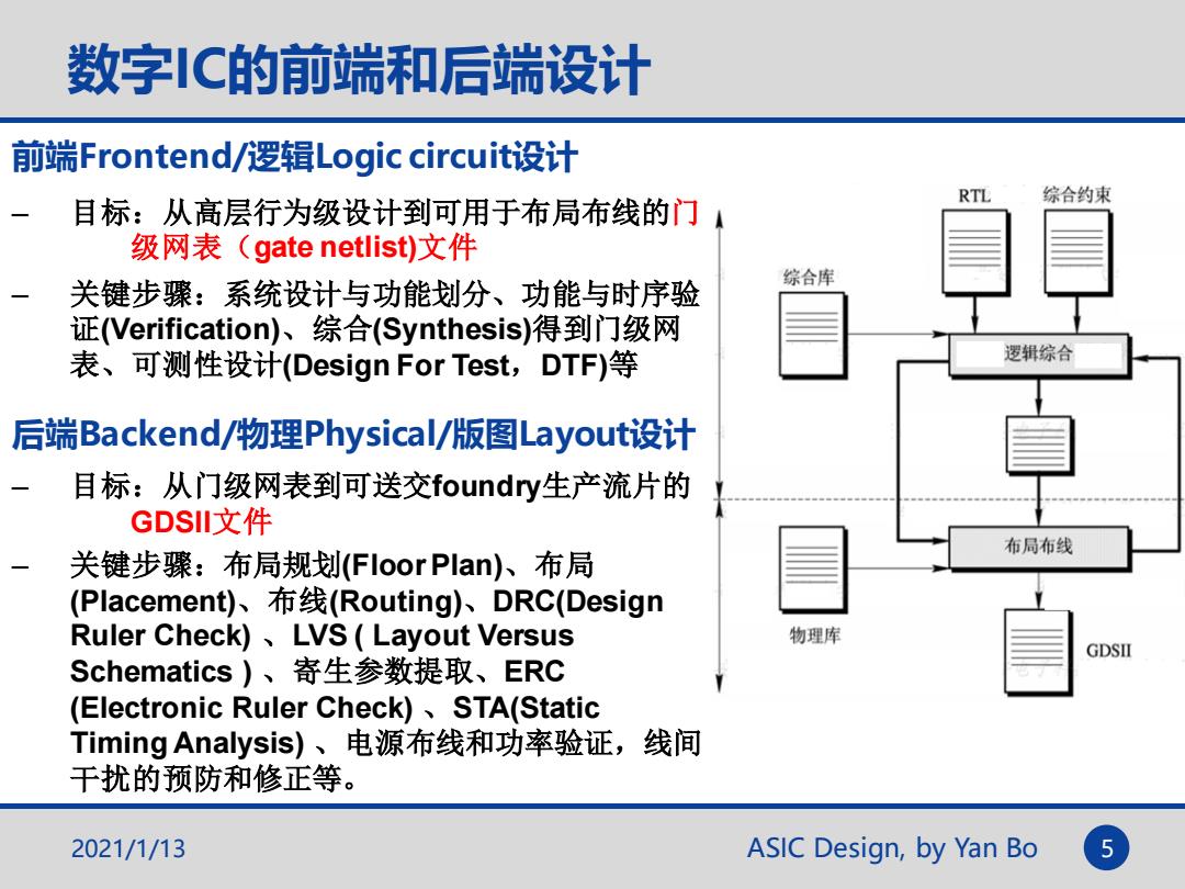
数字IC的前端和后端设计 前端Frontend/逻辑Logic circuit设计 RTL 综合约束 目标:从高层行为级设计到可用于布局布线的门 级网表(gate netlist)文件 综合库 关键步骤:系统设计与功能划分、功能与时序验 证(Verification)、综合(Synthesis)得到门级网 表、可测性设计(Design For Test,DTF)等 逻辑综合 后端Backend/物理Physical/版图Layout设计 目标:从门级网表到可送交foundry生产流片的 GDSl文件 布局布线 关键步骤:布局规划(Floor Plan)、布局 (Placement)、布线(Routing、DRC(Design Ruler Check)LVS(Layout Versus 物理库 GDSII Schematics)、寄生参数提取、ERC (Electronic Ruler Check)STA(Static Timing Analysis)、电源布线和功率验证,线间 干扰的预防和修正等。 2021/1/13 ASIC Design,by Yan Bo 5
ASIC Design, by Yan Bo 数字IC的前端和后端设计 前端Frontend/逻辑Logic circuit设计 – 目标:从高层行为级设计到可用于布局布线的门 级网表(gate netlist)文件 – 关键步骤:系统设计与功能划分、功能与时序验 证(Verification)、综合(Synthesis)得到门级网 表、可测性设计(Design For Test,DTF)等 后端Backend/物理Physical/版图Layout设计 – 目标:从门级网表到可送交foundry生产流片的 GDSII文件 – 关键步骤:布局规划(Floor Plan)、布局 (Placement)、布线(Routing)、DRC(Design Ruler Check) 、LVS ( Layout Versus Schematics ) 、寄生参数提取、ERC (Electronic Ruler Check) 、STA(Static Timing Analysis) 、电源布线和功率验证,线间 干扰的预防和修正等。 2021/1/13 5
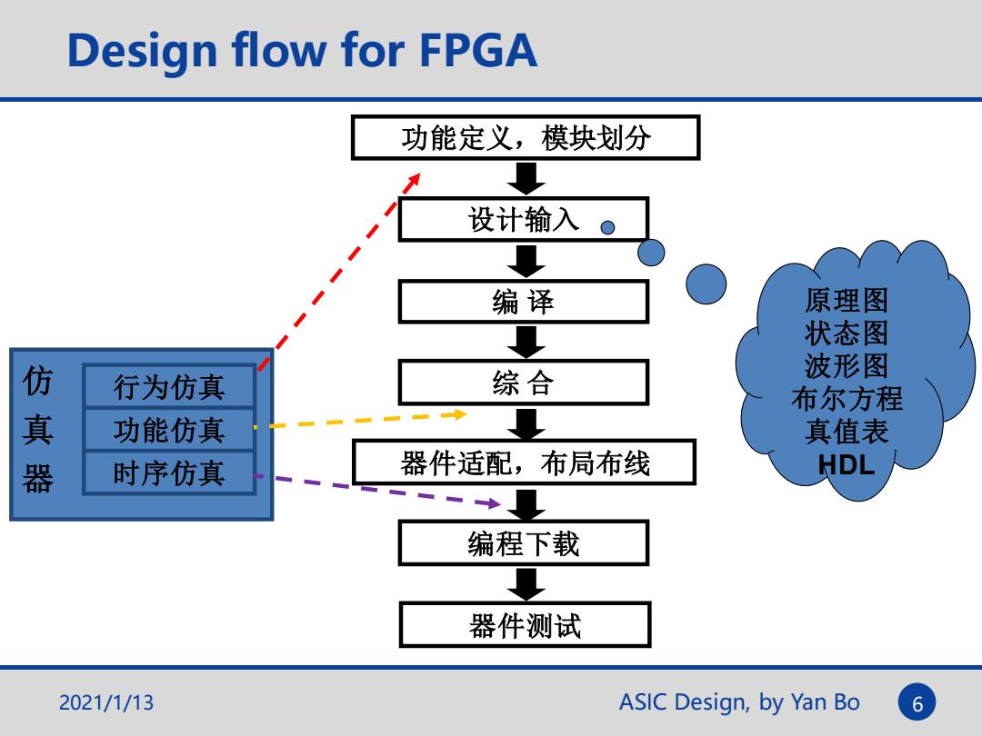
Design flow for FPGA 功能定义,模块划分 设计输入。 编译 原理图 状态图 波形图 行为仿真 综合 真 布尔方程 功能仿真 真值表 时序仿真 器件适配,布局布线 HDL 编程下载 器件测试 2021/1/13 ASIC Design,by Yan Bo 6
ASIC Design, by Yan Bo Design flow for FPGA 设计输入 综 合 编程下载 器件测试 仿 真 器 行为仿真 功能仿真 时序仿真 功能定义,模块划分 编 译 器件适配,布局布线 原理图 状态图 波形图 布尔方程 真值表 HDL 2021/1/13 6

Design flow for Full custom IC 功能定义,模块划分 设计输入 原理图 编译 状态图 波形图 综合 布尔方程 真值表 预布局 HDL 仿真 行为仿真 布局布线 功能仿真 版图生成、版图验证 时序仿真 可测性分析、测试生成 生产加工 硬件仿真 2021/1/13 ASIC Design,by Yan Bo 7
ASIC Design, by Yan Bo Design flow for Full custom IC 综 合 生产加工 硬件仿真 仿 真 器 行为仿真 功能仿真 时序仿真 功能定义,模块划分 编 译 布局布线 原理图 状态图 波形图 布尔方程 真值表 HDL 可测性分析、测试生成 预布局 设计输入 版图生成、版图验证 2021/1/13 7
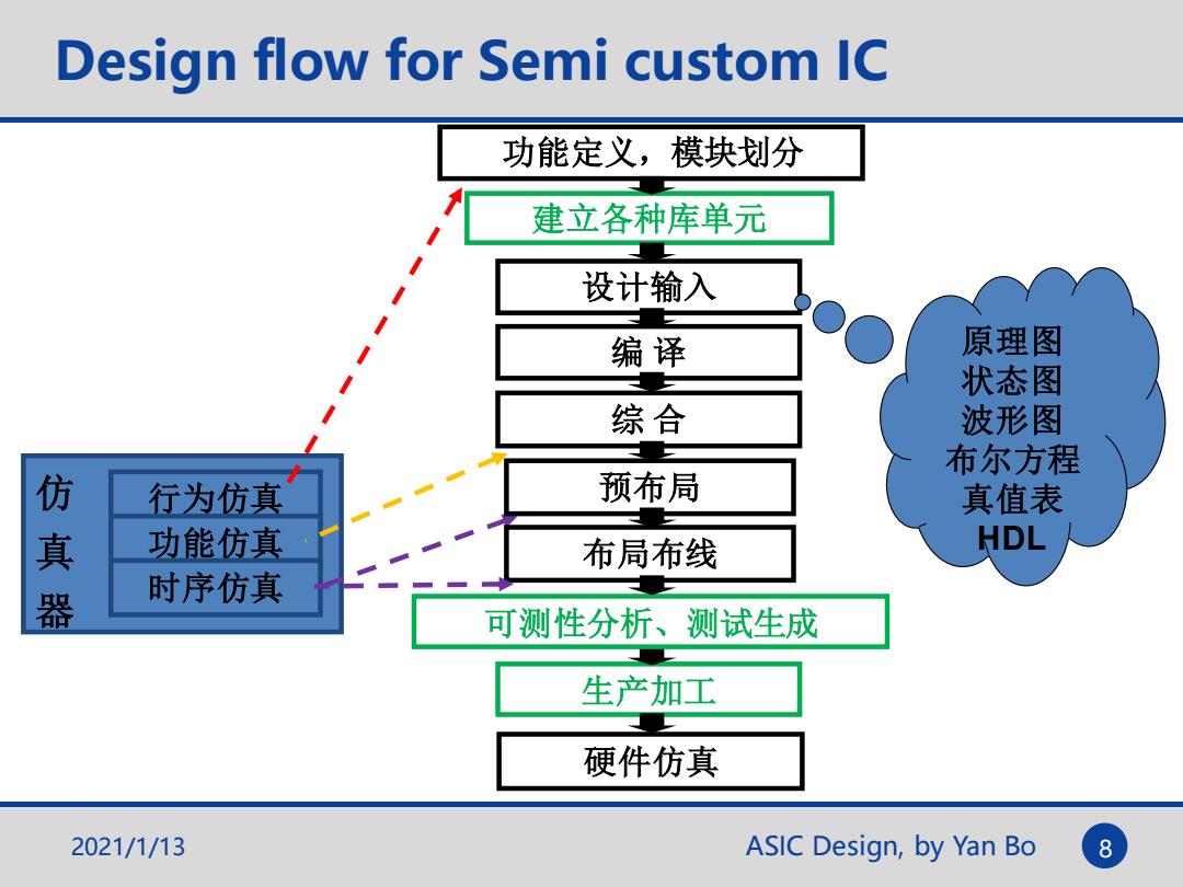
Design flow for Semi custom IC 功能定义,模块划分 建立各种库单元 设计输入 编译 原理图 状态图 综合 波形图 布尔方程 预布局 仿真器 行为仿真 真值表 功能仿真 布局布线 HDL 时序仿真 可测性分析、测试生成 生产加工 硬件仿真 2021/1/13 ASIC Design,by Yan Bo 8
ASIC Design, by Yan Bo Design flow for Semi custom IC 设计输入 综 合 生产加工 硬件仿真 仿 真 器 行为仿真 功能仿真 时序仿真 功能定义,模块划分 编 译 布局布线 原理图 状态图 波形图 布尔方程 真值表 HDL 建立各种库单元 可测性分析、测试生成 预布局 2021/1/13 8
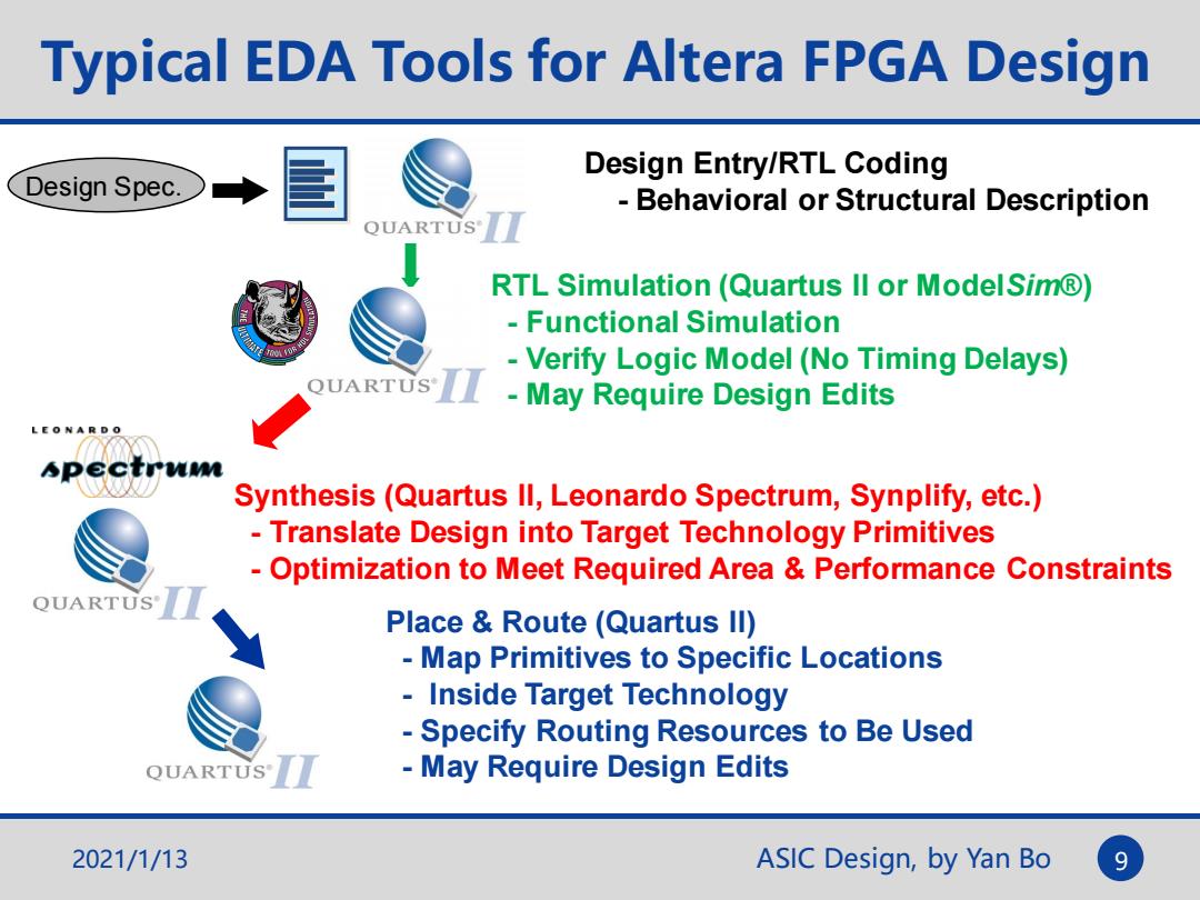
Typical EDA Tools for Altera FPGA Design Design Entry/RTL Coding Design Spec. Behavioral or Structural Description QUARTUS RTL Simulation (Quartus ll or ModelSim@) -Functional Simulation Verify Logic Model (No Timing Delays) QUARTUs-May Require Design Edits LEONARD O Synthesis(Quartus ll,Leonardo Spectrum,Synplify,etc.) Translate Design into Target Technology Primitives -Optimization to Meet Required Area Performance Constraints QUARTUS Place Route (Quartus ll) Map Primitives to Specific Locations Inside Target Technology Specify Routing Resources to Be Used QUARTUS May Require Design Edits 2021/1/13 ASIC Design,by Yan Bo
ASIC Design, by Yan Bo Synthesis (Quartus II, Leonardo Spectrum, Synplify, etc.) - Translate Design into Target Technology Primitives - Optimization to Meet Required Area & Performance Constraints Design Spec. Place & Route (Quartus II) - Map Primitives to Specific Locations - Inside Target Technology - Specify Routing Resources to Be Used - May Require Design Edits Design Entry/RTL Coding - Behavioral or Structural Description RTL Simulation (Quartus II or ModelSim®) - Functional Simulation - Verify Logic Model (No Timing Delays) - May Require Design Edits Typical EDA Tools for Altera FPGA Design 2021/1/13 9
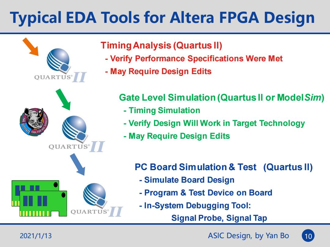
Typical EDA Tools for Altera FPGA Design Timing Analysis(Quartus Il) -Verify Performance Specifications Were Met May Require Design Edits QUARTUS Gate Level Simulation(Quartus ll or ModelSim) Timing Simulation -Verify Design Will Work in Target Technology May Require Design Edits QUARTUS PC Board Simulation Test (Quartus Il) Simulate Board Design Program Test Device on Board QUARTUS In-System Debugging Tool: Signal Probe,Signal Tap 2021/1/13 ASIC Design,by Yan Bo 10
ASIC Design, by Yan Bo Timing Analysis (Quartus II) - Verify Performance Specifications Were Met - May Require Design Edits Gate Level Simulation (Quartus II or ModelSim) - Timing Simulation - Verify Design Will Work in Target Technology - May Require Design Edits PC Board Simulation & Test (Quartus II) - Simulate Board Design - Program & Test Device on Board - In-System Debugging Tool: Signal Probe, Signal Tap Typical EDA Tools for Altera FPGA Design 2021/1/13 10
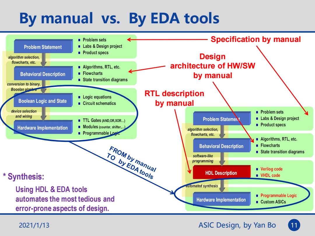
By manual vs.By EDA tools Problem sets Specification by manual Problem Statement Labs Design project Product specs algorithm selection, Design flowcharts,etc. Algorithms,RTL,etc. architecture of HW/SW Behavioral Description Flowcharts State transition diagrams by manual conversion to binary, Booelan alaolra Logic equations RTL description Boolean Logic and State Circuit schematics by manual device selection ■Problem sets and wiring TTL Gates (AND,OR,XOR...) Problem Statemer.t ■Labs&Design project Hardware Implementation Modules (counter,shifter. Product specs algorithm selection, Programmable Logic flowcharts,etc. Algorithms,RTL,etc. Behavioral Description Flowcharts FROM by manual State transition diagrams software-like TO by EDAtools programming Verilog code Synthesis: HDL Description ■VHDL code Using HDL EDA tools automated synthesis automates the most tedious and Programmable Logic Hardware Implementation ■Custom ASICs error-prone aspects of design. 2021/1/13 ASIC Design,by Yan Bo 11
2021/1/13 ASIC Design, by Yan Bo 11 By manual vs. By EDA tools Specification by manual Design architecture of HW/SW by manual RTL description by manual * Synthesis: Using HDL & EDA tools automates the most tedious and error-prone aspects of design
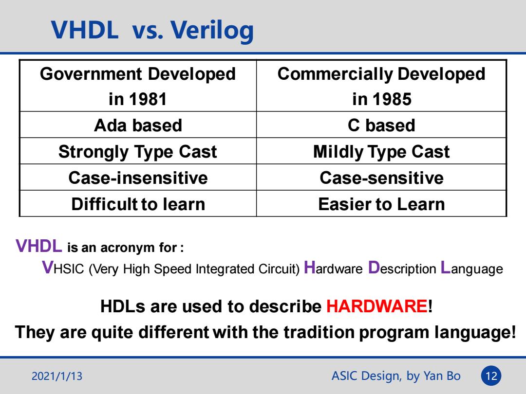
VHDL vs.Verilog Government Developed Commercially Developed in1981 in1985 Ada based C based Strongly Type Cast Mildly Type Cast Case-insensitive Case-sensitive Difficult to learn Easier to Learn VHDL is an acronym for VHSIC (Very High Speed Integrated Circuit)Hardware Description Language HDLs are used to describe HARDWARE! They are quite different with the tradition program language! 2021/1/13 ASIC Design,by Yan Bo 12
ASIC Design, by Yan Bo 12 VHDL vs. Verilog Government Developed in 1981 Commercially Developed in 1985 Ada based C based Strongly Type Cast Mildly Type Cast Case-insensitive Case-sensitive Difficult to learn Easier to Learn VHDL is an acronym for : VHSIC (Very High Speed Integrated Circuit) Hardware Description Language HDLs are used to describe HARDWARE! They are quite different with the tradition program language! 2021/1/13