正在加载图片...

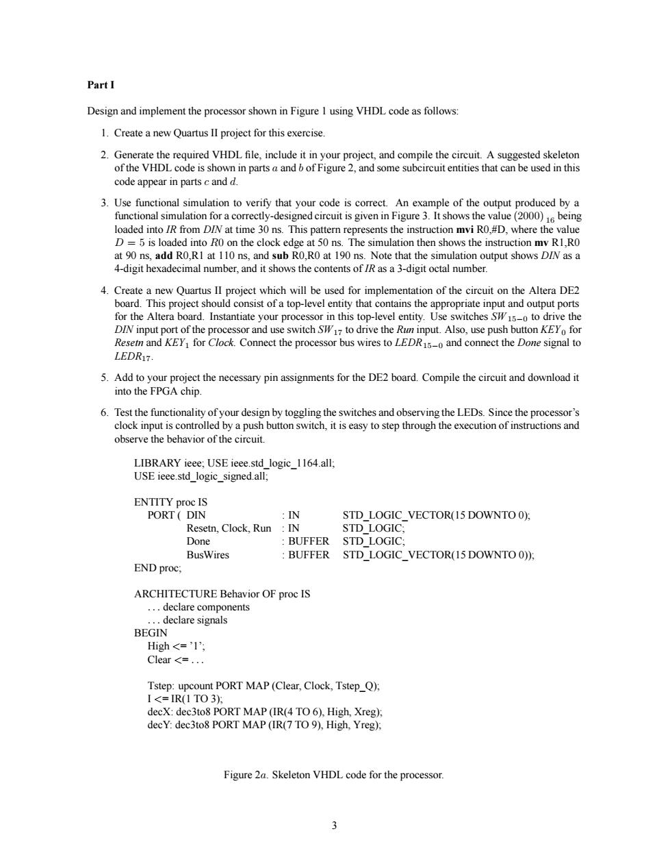
Design and implement the processor shown in Figure 1 using VHDL code as follows: 1.Create a new Quartus II project for this exercise. 3.Use functional simulation to verify that your An of the funetional simulation for a correetly-des loaded into IR from DIN at time 30 ns.This pattern represents the instruction mvi RO.#D.where the value D=5 is l on the clock edge at 50n The simulation then shows the instruction m R1.RO o ns.it sh IR a 13-digi ambe2upushowsDNasg 4 Create a new ouartus ll proiect which will be used for implementation of the circuit on the altera de2 board.This project should consist of a top-level entity that contains the appropriate input and output ports for the Altera be rd.Instantiate your proc ssor in this top-level entity.Use switches S -o to drive th LEDR ,5 n KE) 15-0 5.Add to your project the necessary pin assignments for the DE2 board.Compile the circuit and download it into the FPGA chip. ing the LEDs thefuncdonhh ENTITY proe IS PORT DIN IN STD_LOGIC_VECTOR(15 DOWNTO 0): BusWires BUFFER STD LOGIC VECTOR(15 DOWNTO0)): END proc; ARCHITECTURE Behavior OF proe IS declare cor =1 Tstep:upcount PORT MAP(Clear,Clock,Tstep_Q). Figure 2a.Skeleton VHDL code for the processor. Part I Design and implement the processor shown in Figure 1 using VHDL code as follows: 1. Create a new Quartus II project for this exercise. 2. Generate the required VHDL file, include it in your project, and compile the circuit. A suggested skeleton of the VHDL code is shown in parts a and b of Figure 2, and some subcircuit entities that can be used in this code appear in parts c and d. 3. Use functional simulation to verify that your code is correct. An example of the output produced by a functional simulation for a correctly-designed circuit is given in Figure 3. It shows the value (2000) 16 being loaded into IR from DIN at time 30 ns. This pattern represents the instruction mvi R0,#D, where the value D = 5 is loaded into R0 on the clock edge at 50 ns. The simulation then shows the instruction mv R1,R0 at 90 ns, add R0,R1 at 110 ns, and sub R0,R0 at 190 ns. Note that the simulation output shows DIN as a 4-digit hexadecimal number, and it shows the contents of IR as a 3-digit octal number. 4. Create a new Quartus II project which will be used for implementation of the circuit on the Altera DE2 board. This project should consist of a top-level entity that contains the appropriate input and output ports for the Altera board. Instantiate your processor in this top-level entity. Use switches SW 15−0 to drive the DIN input port of the processor and use switch SW17 to drive the Run input. Also, use push button KEY 0 for Resetn and KEY1 for Clock. Connect the processor bus wires to LEDR15−0 and connect the Done signal to LEDR17. 5. Add to your project the necessary pin assignments for the DE2 board. Compile the circuit and download it into the FPGA chip. 6. Test the functionality of your design by toggling the switches and observing the LEDs. Since the processor’s clock input is controlled by a push button switch, it is easy to step through the execution of instructions and observe the behavior of the circuit. LIBRARY ieee; USE ieee.std_logic_1164.all; USE ieee.std_logic_signed.all; ENTITY proc IS PORT ( DIN : IN STD_LOGIC_VECTOR(15 DOWNTO 0); Resetn, Clock, Run : IN STD_LOGIC; Done : BUFFER STD_LOGIC; BusWires : BUFFER STD_LOGIC_VECTOR(15 DOWNTO 0)); END proc; ARCHITECTURE Behavior OF proc IS ... declare components ... declare signals BEGIN High <= ’1’; Clear <= ... Tstep: upcount PORT MAP (Clear, Clock, Tstep_Q); I <= IR(1 TO 3); decX: dec3to8 PORT MAP (IR(4 TO 6), High, Xreg); decY: dec3to8 PORT MAP (IR(7 TO 9), High, Yreg); Figure 2a. Skeleton VHDL code for the processor. 3