Laboratory Exercise 9 A Simple Processor through the 16-bit wide multiplexer into the various registers,such asOR7and 4.The multiplexer also allows data to be transferred from one register to another.The multiplexer's output wires are called a bus in the this term for wiring that allows data to be transferred from one location in a system to Addition or subtraction is performed by using the multiplexer to first pla e one 16-bit number onto the bus wires and loading this number into register.Once this is done.a second 16-bit number is placed onto the bus Control uni Clear Done Figure 1.A digital system
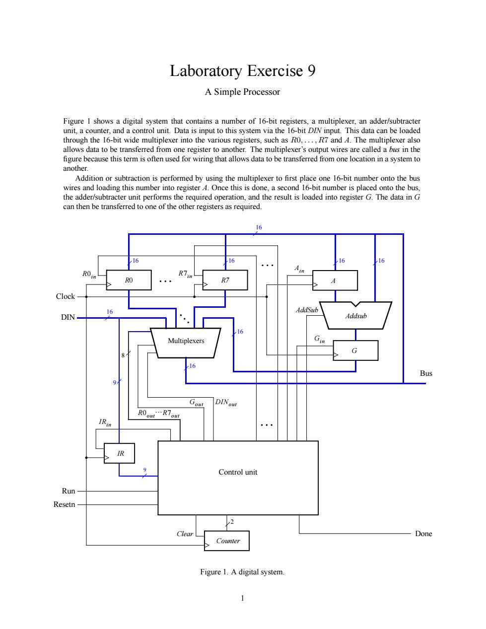
Laboratory Exercise 9 A Simple Processor Figure 1 shows a digital system that contains a number of 16-bit registers, a multiplexer, an adder/subtracter unit, a counter, and a control unit. Data is input to this system via the 16-bit DIN input. This data can be loaded through the 16-bit wide multiplexer into the various registers, such as R0,...,R7 and A. The multiplexer also allows data to be transferred from one register to another. The multiplexer’s output wires are called a bus in the figure because this term is often used for wiring that allows data to be transferred from one location in a system to another. Addition or subtraction is performed by using the multiplexer to first place one 16-bit number onto the bus wires and loading this number into register A. Once this is done, a second 16-bit number is placed onto the bus, the adder/subtracter unit performs the required operation, and the result is loaded into register G. The data in G can then be transferred to one of the other registers as required. Control unit AddSub Ain Gin Run Done 9 16 16 DIN R0in Multiplexers R7in Bus Clock Gout R0out}R7out 16 R0 R7 16 8 DINout 16 IRin Addsub 16 IR 9 A G Counter 2 Clear Resetn 16 16 Figure 1. A digital system. 1
The system can perform different operations in each clock cycle,as governed by the controt This unit determines when particular data is placed onto the bus wires and it controls which of the registers is to be loaded and An.then the multiplexer will place the content Table I lists the instructions that the processor has to support for this exereise.The eft column shows the name p鸣fmrX←仁R门sh the contents6y器一 Operation Function performed mv Rr,Ry mvi Rz,D Rr -D add Rr.Ry Rx-R]+[Ryl sub RE,Ry Rr-[R]-[Ry] Table 1.Instructions performed in the processor re eeded o mode ouctinretohe ind a #D has to be ,take more thanone clock cycle to complete.becaus multiple transfers have to be performed across the bus.The control unit uses the two-bit counter shown in Figure I trol signals that can h that the only control signal asserted in time stepisso this time step is not shown in the table. T T (mv):o Done (mvi):I1 DINRX Done (add) RYout,Gin Gout,RYin (sub):Is RAout,Ain RYout,Gin, Gout,RYin AddSub Done Table 2.Control signals asserted in each instruction/time ster
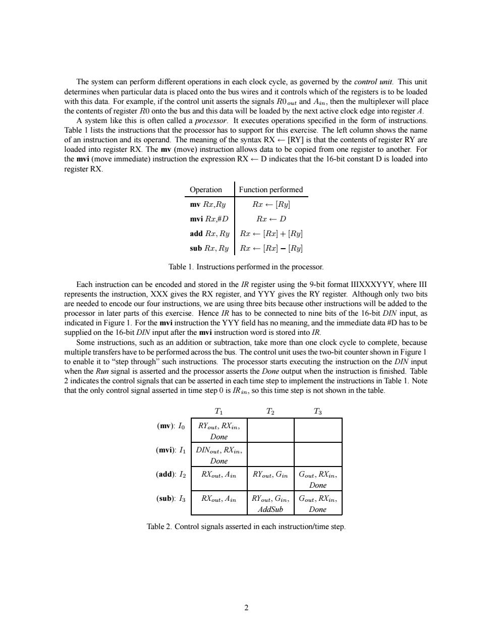
The system can perform different operations in each clock cycle, as governed by the control unit. This unit determines when particular data is placed onto the bus wires and it controls which of the registers is to be loaded with this data. For example, if the control unit asserts the signals R0 out and Ain, then the multiplexer will place the contents of register R0 onto the bus and this data will be loaded by the next active clock edge into register A. A system like this is often called a processor. It executes operations specified in the form of instructions. Table 1 lists the instructions that the processor has to support for this exercise. The left column shows the name of an instruction and its operand. The meaning of the syntax RX ← [RY] is that the contents of register RY are loaded into register RX. The mv (move) instruction allows data to be copied from one register to another. For the mvi (move immediate) instruction the expression RX ← D indicates that the 16-bit constant D is loaded into register RX. Operation Function performed mv Rx,Ry Rx ← [Ry] mvi Rx,#D Rx ← D add Rx, Ry Rx ← [Rx]+[Ry] sub Rx, Ry Rx ← [Rx] − [Ry] Table 1. Instructions performed in the processor. Each instruction can be encoded and stored in the IR register using the 9-bit format IIIXXXYYY, where III represents the instruction, XXX gives the RX register, and YYY gives the RY register. Although only two bits are needed to encode our four instructions, we are using three bits because other instructions will be added to the processor in later parts of this exercise. Hence IR has to be connected to nine bits of the 16-bit DIN input, as indicated in Figure 1. For the mvi instruction the YYY field has no meaning, and the immediate data #D has to be supplied on the 16-bit DIN input after the mvi instruction word is stored into IR. Some instructions, such as an addition or subtraction, take more than one clock cycle to complete, because multiple transfers have to be performed across the bus. The control unit uses the two-bit counter shown in Figure 1 to enable it to “step through” such instructions. The processor starts executing the instruction on the DIN input when the Run signal is asserted and the processor asserts the Done output when the instruction is finished. Table 2 indicates the control signals that can be asserted in each time step to implement the instructions in Table 1. Note that the only control signal asserted in time step 0 is IRin, so this time step is not shown in the table. T1 T2 T3 (mv): I0 RYout, RXin, Done (mvi): I1 DINout, RXin, Done (add): I2 RXout, Ain RYout, Gin Gout, RXin, Done (sub): I3 RXout, Ain RYout, Gin, Gout, RXin, AddSub Done Table 2. Control signals asserted in each instruction/time step. 2
Design and implement the processor shown in Figure 1 using VHDL code as follows: 1.Create a new Quartus II project for this exercise. 3.Use functional simulation to verify that your An of the funetional simulation for a correetly-des loaded into IR from DIN at time 30 ns.This pattern represents the instruction mvi RO.#D.where the value D=5 is l on the clock edge at 50n The simulation then shows the instruction m R1.RO o ns.it sh IR a 13-digi ambe2upushowsDNasg 4 Create a new ouartus ll proiect which will be used for implementation of the circuit on the altera de2 board.This project should consist of a top-level entity that contains the appropriate input and output ports for the Altera be rd.Instantiate your proc ssor in this top-level entity.Use switches S -o to drive th LEDR ,5 n KE) 15-0 5.Add to your project the necessary pin assignments for the DE2 board.Compile the circuit and download it into the FPGA chip. ing the LEDs thefuncdonhh ENTITY proe IS PORT DIN IN STD_LOGIC_VECTOR(15 DOWNTO 0): BusWires BUFFER STD LOGIC VECTOR(15 DOWNTO0)): END proc; ARCHITECTURE Behavior OF proe IS declare cor =1 Tstep:upcount PORT MAP(Clear,Clock,Tstep_Q). Figure 2a.Skeleton VHDL code for the processor
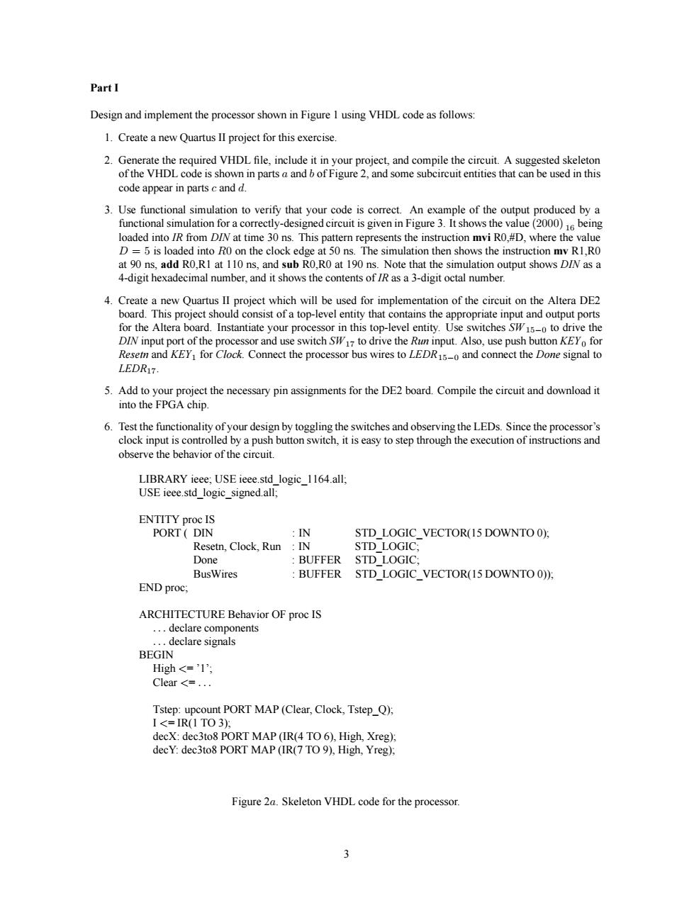
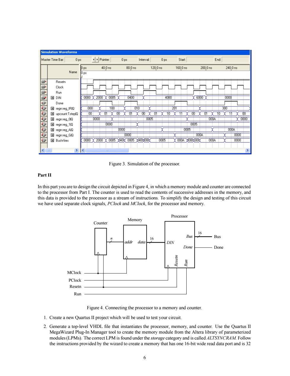
Part I Design and implement the processor shown in Figure 1 using VHDL code as follows: 1. Create a new Quartus II project for this exercise. 2. Generate the required VHDL file, include it in your project, and compile the circuit. A suggested skeleton of the VHDL code is shown in parts a and b of Figure 2, and some subcircuit entities that can be used in this code appear in parts c and d. 3. Use functional simulation to verify that your code is correct. An example of the output produced by a functional simulation for a correctly-designed circuit is given in Figure 3. It shows the value (2000) 16 being loaded into IR from DIN at time 30 ns. This pattern represents the instruction mvi R0,#D, where the value D = 5 is loaded into R0 on the clock edge at 50 ns. The simulation then shows the instruction mv R1,R0 at 90 ns, add R0,R1 at 110 ns, and sub R0,R0 at 190 ns. Note that the simulation output shows DIN as a 4-digit hexadecimal number, and it shows the contents of IR as a 3-digit octal number. 4. Create a new Quartus II project which will be used for implementation of the circuit on the Altera DE2 board. This project should consist of a top-level entity that contains the appropriate input and output ports for the Altera board. Instantiate your processor in this top-level entity. Use switches SW 15−0 to drive the DIN input port of the processor and use switch SW17 to drive the Run input. Also, use push button KEY 0 for Resetn and KEY1 for Clock. Connect the processor bus wires to LEDR15−0 and connect the Done signal to LEDR17. 5. Add to your project the necessary pin assignments for the DE2 board. Compile the circuit and download it into the FPGA chip. 6. Test the functionality of your design by toggling the switches and observing the LEDs. Since the processor’s clock input is controlled by a push button switch, it is easy to step through the execution of instructions and observe the behavior of the circuit. LIBRARY ieee; USE ieee.std_logic_1164.all; USE ieee.std_logic_signed.all; ENTITY proc IS PORT ( DIN : IN STD_LOGIC_VECTOR(15 DOWNTO 0); Resetn, Clock, Run : IN STD_LOGIC; Done : BUFFER STD_LOGIC; BusWires : BUFFER STD_LOGIC_VECTOR(15 DOWNTO 0)); END proc; ARCHITECTURE Behavior OF proc IS ... declare components ... declare signals BEGIN High <= ’1’; Clear <= ... Tstep: upcount PORT MAP (Clear, Clock, Tstep_Q); I <= IR(1 TO 3); decX: dec3to8 PORT MAP (IR(4 TO 6), High, Xreg); decY: dec3to8 PORT MAP (IR(7 TO 9), High, Yreg); Figure 2a. Skeleton VHDL code for the processor. 3
sPROCESS () pecify initial values CASE Tstep_QIS WHEN "00*- -store DIN in IR as long as Tstep_Q=0 WHEN -OI --define signals in time step TI cAsEus define signals in time stepT2 CASEIIS .CASE -define signals in time step T3 CASEIIS END CASE reg_0:regn PORT MAP(BusWires,Rin(0),Clock,RO), :define the buiser registers nd Figure 2b.Skeleton VHDL code for the processor. LIBRARY ieee; ENTITY upcount IS PORT(Clear,Clock IN STD_LOGIC OUT STD_LOGIC_VECTOR(I DOWNTO 0)): BEGNAL CoSTD LOGIC VECTORLI DONWNTOO ARCHITECTURE Behavior OF upcount IS IF (Clock'EVENT AND Clock='1')THEN Count <Count+1; END IF; Q=Count END Behavior; Figure 2c.Subcircuit entities for use in the processor
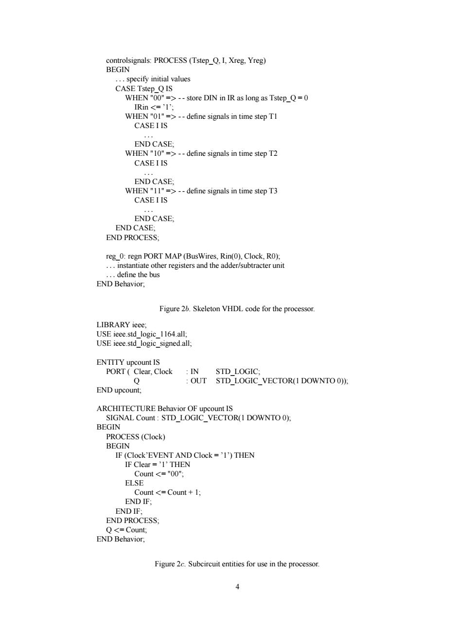
controlsignals: PROCESS (Tstep_Q, I, Xreg, Yreg) BEGIN ... specify initial values CASE Tstep_Q IS WHEN "00" => - - store DIN in IR as long as Tstep_Q = 0 IRin - - define signals in time step T1 CASE I IS ... END CASE; WHEN "10" => - - define signals in time step T2 CASE I IS ... END CASE; WHEN "11" => - - define signals in time step T3 CASE I IS ... END CASE; END CASE; END PROCESS; reg_0: regn PORT MAP (BusWires, Rin(0), Clock, R0); ... instantiate other registers and the adder/subtracter unit ... define the bus END Behavior; Figure 2b. Skeleton VHDL code for the processor. LIBRARY ieee; USE ieee.std_logic_1164.all; USE ieee.std_logic_signed.all; ENTITY upcount IS PORT ( Clear, Clock : IN STD_LOGIC; Q : OUT STD_LOGIC_VECTOR(1 DOWNTO 0)); END upcount; ARCHITECTURE Behavior OF upcount IS SIGNAL Count : STD_LOGIC_VECTOR(1 DOWNTO 0); BEGIN PROCESS (Clock) BEGIN IF (Clock’EVENT AND Clock = ’1’) THEN IF Clear = ’1’ THEN Count <= "00"; ELSE Count <= Count + 1; END IF; END IF; END PROCESS; Q <= Count; END Behavior; Figure 2c. Subcircuit entities for use in the processor. 4
LIBRARY ieee: USE ieee.std_logic_1164.all; IN STD LOGIC VECTORO2 DOWNTO O) En:IN STD LOGIC: END dectos. OUT STD LOGIC VECTOR(OTO7)): ARCHITECTURE Behavior OF dec3to8 IS BEGIN (W.En) IF En='1'THEN CASE WIS WHEN010=YY<-00000001 END CASE; ELSE END PROCESS. END Behavior: std logic 1164.all: ENTITY regn IS ORE(n:INTEGER =16月 STD_LOGIC_VECTOR(n-1 DOWNTO 0): Rin,Clock .IN STD LOGIC: Q BUFFER STD_LOGIC_VECTOR(n-1 DOWNTO 0)): END regn, ARCHITECTURE Behavior OF regn IS BEGIN PROCESS(Clock) Q<■R D IF: END PROCESS END Behavior:. Figure 2d.Subcircuit entities for use in the processor. 5
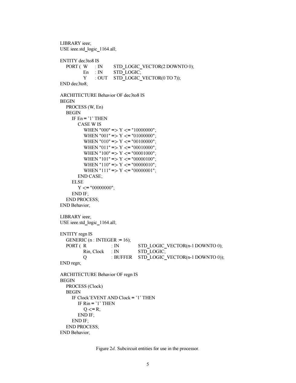
LIBRARY ieee; USE ieee.std_logic_1164.all; ENTITY dec3to8 IS PORT ( W : IN STD_LOGIC_VECTOR(2 DOWNTO 0); En : IN STD_LOGIC; Y : OUT STD_LOGIC_VECTOR(0 TO 7)); END dec3to8; ARCHITECTURE Behavior OF dec3to8 IS BEGIN PROCESS (W, En) BEGIN IF En = ’1’ THEN CASE W IS WHEN "000" => Y Y Y Y Y Y Y Y <= "00000001"; END CASE; ELSE Y <= "00000000"; END IF; END PROCESS; END Behavior; LIBRARY ieee; USE ieee.std_logic_1164.all; ENTITY regn IS GENERIC (n : INTEGER := 16); PORT ( R : IN STD_LOGIC_VECTOR(n-1 DOWNTO 0); Rin, Clock : IN STD_LOGIC; Q : BUFFER STD_LOGIC_VECTOR(n-1 DOWNTO 0)); END regn; ARCHITECTURE Behavior OF regn IS BEGIN PROCESS (Clock) BEGIN IF Clock’EVENT AND Clock = ’1’ THEN IF Rin = ’1’ THEN Q <= R; END IF; END IF; END PROCESS; END Behavior; Figure 2d. Subcircuit entities for use in the processor. 5
0p3 0 Sta End 400m 200n 600n 2400n Name X10 02a00X00500m5⑩0m5 Figure 3.Simulation of the processo Part II In this part you are to de n Fig whichamemory moduleand 1 this data is provided to the processor as a stream of instruction.Tosimplify the design and testing of this circuit we have used separate clock signals,PClock and MClock,for the processor and memory. MClock PClock Resetn Run Figure 4.Connecting the processor to a memory and counter 1.Create a new Quartus II project which will be used to test your circuit 2 Generate a ton-level vHDL file that instantiates the d counter Use the ouartus I Megawizard Plug-n Manager tool to create the memory module from the Altera library of parameterized modules(LPMs).The comrect LPM is found under the storage eategory and is called ALTSYNCRAM Follow the instructions provided by the wizard to create a memory that has one 16-bit wide read data port and is 32
Figure 3. Simulation of the processor. Part II In this part you are to design the circuit depicted in Figure 4, in which a memory module and counter are connected to the processor from Part I. The counter is used to read the contents of successive addresses in the memory, and this data is provided to the processor as a stream of instructions. To simplify the design and testing of this circuit we have used separate clock signals, PClock and MClock, for the processor and memory. Counter n Resetn MClock Memory 16 addr data Processor 16 DIN Bus Resetn Run Done Run Bus Done PClock Figure 4. Connecting the processor to a memory and counter. 1. Create a new Quartus II project which will be used to test your circuit. 2. Generate a top-level VHDL file that instantiates the processor, memory, and counter. Use the Quartus II MegaWizard Plug-In Manager tool to create the memory module from the Altera library of parameterized modules (LPMs). The correct LPM is found under the storage category and is called ALTSYNCRAM. Follow the instructions provided by the wizard to create a memory that has one 16-bit wide read data port and is 32 6

vords deen The first s of the wizard is shown in figure 5 Since this m includes a register for synchronously loading addresses.This register is required due to the design of the memory resources on the Cyclone II FPGA;account for the clocking of this address register in your design To place processor instructions into the memory,you need to specify initial values that should be stored in the memory once your circuit has been programmed into the FPGA chip.This can be done by telling the ze the memory using the cont a me screen which then has to he created in the direc ins the Qua ect Ilse the Quartus on-n Helpto lea about the format of theand createthat hasr instructions to test your circuit. 3epesiaoeaeticlBarctasedpopeodofeoMandamd pin loca e e for MClock,and useKEY for PClock Connect the processor bus wires toRand connect the Done signal to LEDR17. 5.Compile the circuit and download it into the FPGA chip. MegaWizard Plug-n Manager-ALTSYNCRAM [page 1 of Curertly selected device famiy:Cclonell H Wih one read port [ROM model With two read/write ports [Tue dual-port mode) inst_mem dess时4.01 As a numbet of words Block Type:A Figure 5.ALTSYNCRAM configuration. 7
words deep. The first screen of the wizard is shown in Figure 5. Since this memory has only a read port, and no write port, it is called a synchronous read-only memory (synchronous ROM). Note that the memory includes a register for synchronously loading addresses. This register is required due to the design of the memory resources on the Cyclone II FPGA; account for the clocking of this address register in your design. To place processor instructions into the memory, you need to specify initial values that should be stored in the memory once your circuit has been programmed into the FPGA chip. This can be done by telling the wizard to initialize the memory using the contents of a memory initialization file (MIF). The appropriate screen of the MegaWizard Plug-In Manager tool is illustrated in Figure 6. We have specified a file named inst_mem.mif, which then has to be created in the directory that contains the Quartus II project. Use the Quartus II on-line Help to learn about the format of the MIF file and create a file that has enough processor instructions to test your circuit. 3. Use functional simulation to test the circuit. Ensure that data is read properly out of the ROM and executed by the processor. 4. Make sure your project includes the necessary port names and pin location assignments to implement the circuit on the DE2 board. Use switch SW17 to drive the processor’s Run input, use KEY0 for Resetn, use KEY1 for MClock, and use KEY2 for PClock. Connect the processor bus wires to LEDR15−0 and connect the Done signal to LEDR17. 5. Compile the circuit and download it into the FPGA chip. 6. Test the functionality of your design by toggling the switches and observing the LEDs. Since the circuit’s clock inputs are controlled by push button switches, it is easy to step through the execution of instructions and observe the behavior of the circuit. Figure 5. ALTSYNCRAM configuration. 7

MegaWizard Plug-In Manager-ALTSYNCRAM [page 7 of B] cily the inal contert of the memoty? Yes,use this fle for the me Fle name inst mem re54.0 15.0 ck Type:Au0 Documentation. Cancel Back Nest>Finith Figure 6.Specifying a memory initialization file(MIF) Enhanced Processor enhancements involve adding new instructions to the processor and the programs that the processor executes are Since th beyond the scope of some logic design courses,they are described n a subsequent exercise avail Copyright2006 Altera Corporation
Figure 6. Specifying a memory initialization file (MIF). Enhanced Processor It is possible to enhance the capability of the processor so that the counter in Figure 4 is no longer needed, and so that the processor has the ability to perform read and write operations using memory or other devices. These enhancements involve adding new instructions to the processor and the programs that the processor executes are therefore more complex. Since these steps are beyond the scope of some logic design courses, they are described in a subsequent lab exercise available from Altera. Copyright c 2006 Altera Corporation. 8�