正在加载图片...

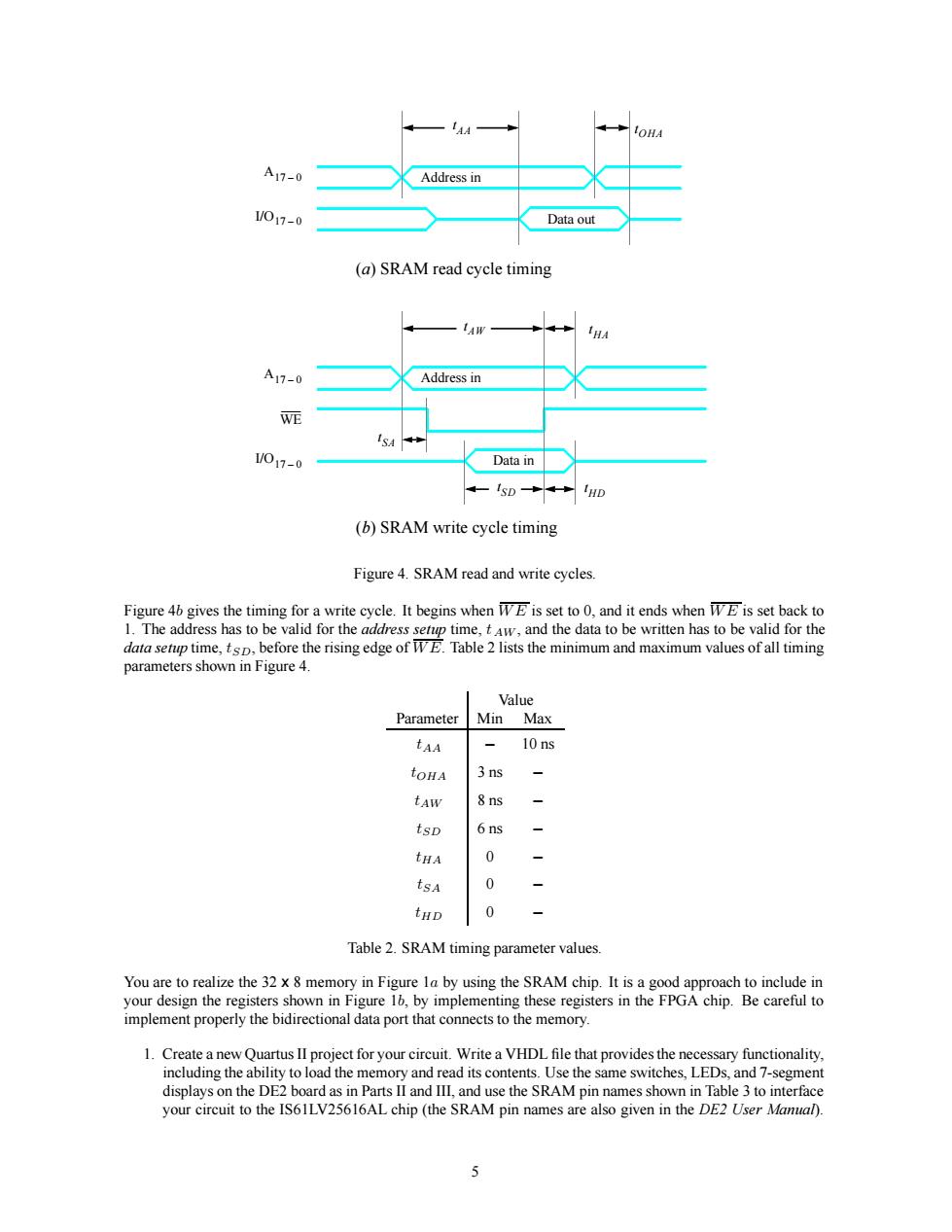
A7-0 Address in V017-0 Data out (a)SRAM read cycle timing A17-0 Address in WE Data in +IsD HD (b)SRAM write cycle timing Figure 4.SRAM read and write cycles. de when set hack t data sep time,s before the rising edge of Table2 lists the minimum and maximum values of all timing parameters shown in Figure 4. Value Parameter Min Max -10ns toHA 3 ns tAW 8ns 6ns tHA 0 tsA 0 八 0 、 Table 2.SRAM timing parameter values your design the 1.Create anew Quartus lI project for your circuit.Write a VHDL file that provides the nece ary functionality -segmenData out Address in t AA t OHA (a) SRAM read cycle timing Address in t AW t HA (b) SRAM write cycle timing Data in tHD t SD t SA A17 0 – I/O17 0 – A17 0 – I/O17 0 – WE Figure 4. SRAM read and write cycles. Figure 4b gives the timing for a write cycle. It begins when W E is set to 0, and it ends when W E is set back to 1. The address has to be valid for the address setup time, t AW , and the data to be written has to be valid for the data setup time, tSD, before the rising edge of W E. Table 2 lists the minimum and maximum values of all timing parameters shown in Figure 4. Value Parameter Min Max tAA − 10 ns tOHA 3 ns − tAW 8 ns − tSD 6 ns − tHA 0 − tSA 0 − tHD 0 − Table 2. SRAM timing parameter values. You are to realize the 32 x 8 memory in Figure 1a by using the SRAM chip. It is a good approach to include in your design the registers shown in Figure 1b, by implementing these registers in the FPGA chip. Be careful to implement properly the bidirectional data port that connects to the memory. 1. Create a new Quartus II project for your circuit. Write a VHDL file that provides the necessary functionality, including the ability to load the memory and read its contents. Use the same switches, LEDs, and 7-segment displays on the DE2 board as in Parts II and III, and use the SRAM pin names shown in Table 3 to interface your circuit to the IS61LV25616AL chip (the SRAM pin names are also given in the DE2 User Manual). 5