正在加载图片...
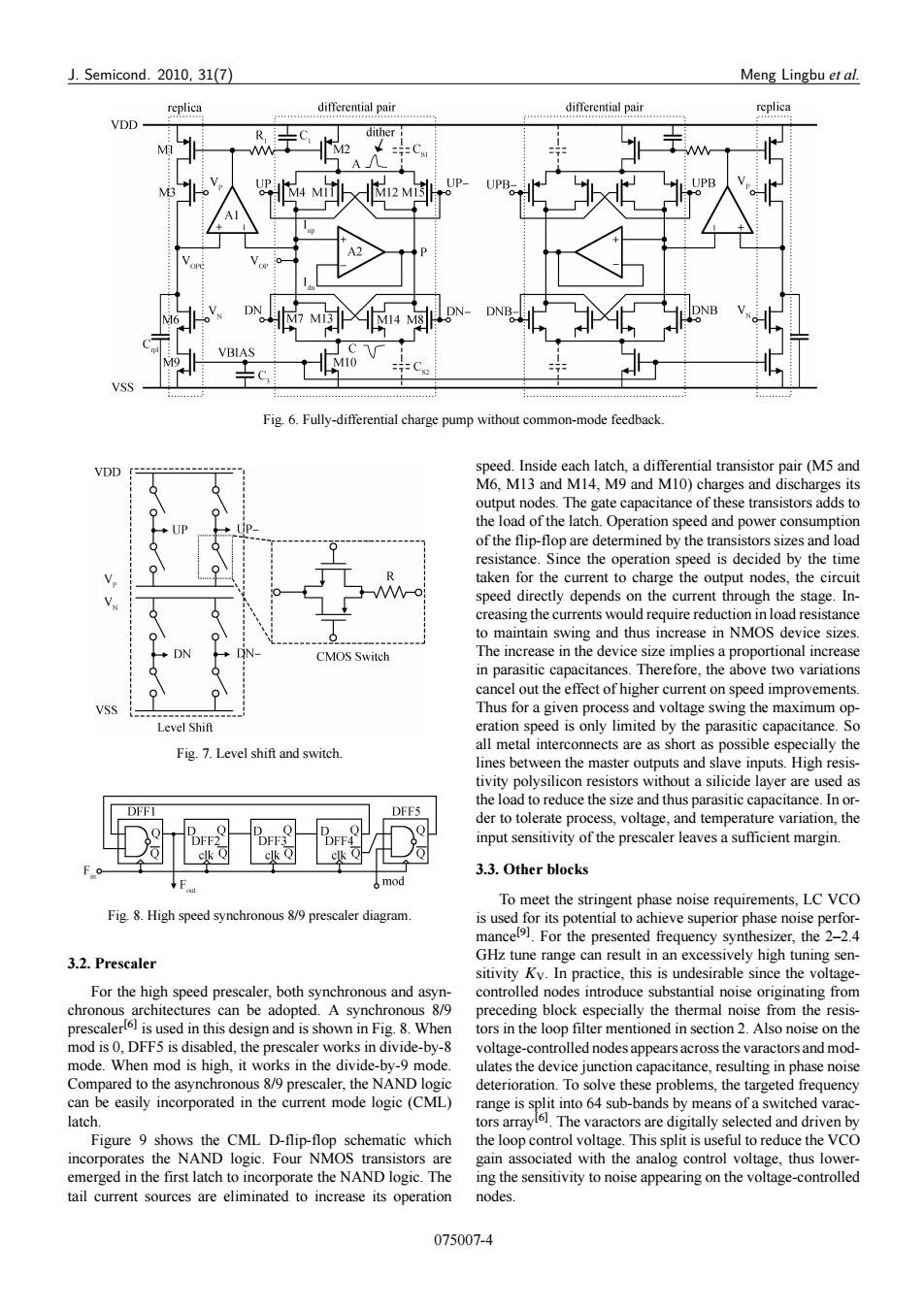
J.Semicond.2010,31(7) Meng Lingbu et al. replica differential pair differental pair replica VDD. R dither PE VBIAS VSS Fig.6.Fully-differential charge pump without common-mode feedback. VDD speed.Inside each latch,a differential transistor pair(M5 and M6.M13 and M14.M9 and M10)charges and discharges its output nodes.The gate capacitance of these transistors adds to the load of the latch.Operation speed and power consumption of the flip-flop are determined by the transistors sizes and load resistance.Since the operation speed is decided by the time taken for the current to charge the output nodes,the circuit speed directly depends on the current through the stage.In- creasing the currents would require reduction in load resistance ● to maintain swing and thus increase in NMOS device sizes. CMOS Switch The increase in the device size implies a proportional increase in parasitic capacitances.Therefore,the above two variations cancel out the effect of higher current on speed improvements. VSS Thus for a given process and voltage swing the maximum op- Level Shift eration speed is only limited by the parasitic capacitance.So Fig.7.Level shift and switch all metal interconnects are as short as possible especially the lines between the master outputs and slave inputs.High resis- tivity polysilicon resistors without a silicide layer are used as the load to reduce the size and thus parasitic capacitance.In or- der to tolerate process,voltage,and temperature variation,the input sensitivity of the prescaler leaves a sufficient margin. 3.3.Other blocks To meet the stringent phase noise requirements,LC VCO Fig.8.High speed synchronous 8/9 prescaler diagram. is used for its potential to achieve superior phase noise perfor- mancel91.For the presented frequency synthesizer,the 2-2.4 3.2.Prescaler GHz tune range can result in an excessively high tuning sen- sitivity Kv.In practice,this is undesirable since the voltage- For the high speed prescaler,both synchronous and asyn- controlled nodes introduce substantial noise originating from chronous architectures can be adopted.A synchronous 8/9 preceding block especially the thermal noise from the resis- prescaler]is used in this design and is shown in Fig.8.When tors in the loop filter mentioned in section 2.Also noise on the mod is 0,DFF5 is disabled,the prescaler works in divide-by-8 voltage-controlled nodes appears across the varactors and mod- mode.When mod is high,it works in the divide-by-9 mode. ulates the device junction capacitance,resulting in phase noise Compared to the asynchronous 8/9 prescaler,the NAND logic deterioration.To solve these problems,the targeted frequency can be easily incorporated in the current mode logic (CML) range is split into 64 sub-bands by means of a switched varac- latch. tors array.The varactors are digitally selected and driven by Figure 9 shows the CML D-flip-flop schematic which the loop control voltage.This split is useful to reduce the VCO incorporates the NAND logic.Four NMOS transistors are gain associated with the analog control voltage,thus lower- emerged in the first latch to incorporate the NAND logic.The ing the sensitivity to noise appearing on the voltage-controlled tail current sources are eliminated to increase its operation nodes. 075007-4J. Semicond. 2010, 31(7) Meng Lingbu et al. Fig. 6. Fully-differential charge pump without common-mode feedback. Fig. 7. Level shift and switch. Fig. 8. High speed synchronous 8/9 prescaler diagram. 3.2. Prescaler For the high speed prescaler, both synchronous and asynchronous architectures can be adopted. A synchronous 8/9 prescalerŒ6 is used in this design and is shown in Fig. 8. When mod is 0, DFF5 is disabled, the prescaler works in divide-by-8 mode. When mod is high, it works in the divide-by-9 mode. Compared to the asynchronous 8/9 prescaler, the NAND logic can be easily incorporated in the current mode logic (CML) latch. Figure 9 shows the CML D-flip-flop schematic which incorporates the NAND logic. Four NMOS transistors are emerged in the first latch to incorporate the NAND logic. The tail current sources are eliminated to increase its operation speed. Inside each latch, a differential transistor pair (M5 and M6, M13 and M14, M9 and M10) charges and discharges its output nodes. The gate capacitance of these transistors adds to the load of the latch. Operation speed and power consumption of the flip-flop are determined by the transistors sizes and load resistance. Since the operation speed is decided by the time taken for the current to charge the output nodes, the circuit speed directly depends on the current through the stage. Increasing the currents would require reduction in load resistance to maintain swing and thus increase in NMOS device sizes. The increase in the device size implies a proportional increase in parasitic capacitances. Therefore, the above two variations cancel out the effect of higher current on speed improvements. Thus for a given process and voltage swing the maximum operation speed is only limited by the parasitic capacitance. So all metal interconnects are as short as possible especially the lines between the master outputs and slave inputs. High resistivity polysilicon resistors without a silicide layer are used as the load to reduce the size and thus parasitic capacitance. In order to tolerate process, voltage, and temperature variation, the input sensitivity of the prescaler leaves a sufficient margin. 3.3. Other blocks To meet the stringent phase noise requirements, LC VCO is used for its potential to achieve superior phase noise performanceŒ9. For the presented frequency synthesizer, the 2–2.4 GHz tune range can result in an excessively high tuning sensitivity KV. In practice, this is undesirable since the voltagecontrolled nodes introduce substantial noise originating from preceding block especially the thermal noise from the resistors in the loop filter mentioned in section 2. Also noise on the voltage-controlled nodes appears across the varactors and modulates the device junction capacitance, resulting in phase noise deterioration. To solve these problems, the targeted frequency range is split into 64 sub-bands by means of a switched varactors arrayŒ6. The varactors are digitally selected and driven by the loop control voltage. This split is useful to reduce the VCO gain associated with the analog control voltage, thus lowering the sensitivity to noise appearing on the voltage-controlled nodes. 075007-4