正在加载图片...
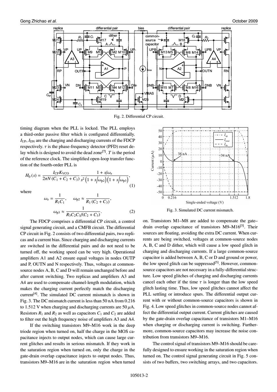
Gong Zhichao et al. October 2009 differ ential pair bias differential pair replica dither common- source M18 22 8eew过5 UPB M13M5 M6M14 OUTH OUTN 14M ON-M15 M小48w VN Fig.2.Differential CP circuit. timing diagram when the PLL is locked.The PLL employs a third-order passive filter which is configured differentially. 50 40 lup,IpN are the charging and discharging currents of the FDCP 30 respectively.r is the phase-frequency detector(PFD)reset de- lay which is designed to avoid the dead zonel7.T is the period 10 38:nA. 34 of the reference clock.The simplified open-loop transfer func- tion of the fourth-order PLL is -10 IcpKvCo 1+s/z Ho ()=2N(C+C+C)+sp2)(1+) -20… -30· 1) 40 where -50 1 Wz= RC1’ p2≈R1(C2+C3 00.216 1.512 Single-ended voltage (V) wp3≈RC2C3/C2+C3) (2) Fig.3.Simulated DC current mismatch. The FDCP comprises a differential CP circuit,a control on.Transistors MI-M8 are added to compensate the gate- signal generating circuit,and a CMFB circuit.The differential drain overlap capacitance of transistors M9-M16151.Their CP circuit in Fig.2 consists of two differential pairs,two repli- sources are floating,avoiding the extra DC current.When cur- cas and a current bias.Since charging and discharging currents rents are being switched,voltages at common-source nodes are switched in the differential pairs and do not need to be A.B.C and D dither,which will cause a low speed glitch in turned off,the working speed can be very high.Operational charging and discharging currents.If a large common-source amplifiers Al and A2 ensure equal voltages in nodes OUTP capacitor is added between A,B,C or D and ground or power, and P.OUTN and N respectively.Thus,voltages at common- the low speed glitch can be suppressedls1.However,common- source nodes A,B,C and D will remain unchanged before and source capacitors are not necessary in a fully-differential struc- after current switching.Two replicas and amplifiers A3 and ture.Low speed glitches of charging and discharging currents A4 are used to compensate channel-length modulation,which cancel each other if the time r is longer than the low speed makes the charging current perfectly match the discharging glitch lasting time.Thus,low speed glitches cannot affect the current!4).The simulated DC current mismatch is shown in PLL settling or introduce spurs.The differential output cur- Fig.3.The DC mismatch current is less than 50 nA from 0.216 rent with or without common-source capacitors is shown in to 1.512 V when charging and discharging currents are 50 uA. Fig.4.Low speed glitches in common-source nodes cannot af- Resistors R and R2 as well as capacitors Ci and C2 are added fect the differential output current.Current glitches are caused to filter out the high frequency noise of amplifiers A3 and A4. by the gate-drain overlap capacitance of transistors MI-M16 If the switching transistors M9-M16 work in the deep when charging or discharging current is switching.Further- triode region when turned on,half the charge in the MOS ca- more,common-source capacitors may increase the noise con- pacitance injects to output nodes,which can cause large cur- tribution from transistors M9-M16. rent glitches and results in serious mismatch.If they work in The control signal of transistors M9-M16 should be care- the saturation region when turned on,only the charge in the fully designed to ensure working in the saturation region when gate-drain overlap capacitance injects to output nodes.Thus, turned on.The control signal generating circuit in Fig.5 con- transistors M9-M16 are in the saturation region when turned sists of two buffers,two switching arrays,and two capacitors. 105013-2Gong Zhichao et al. October 2009 Fig. 2. Differential CP circuit. timing diagram when the PLL is locked. The PLL employs a third-order passive filter which is configured differentially. IUP, IDN are the charging and discharging currents of the FDCP respectively. τ is the phase-frequency detector (PFD) reset delay which is designed to avoid the dead zone[7] . T is the period of the reference clock. The simplified open-loop transfer function of the fourth-order PLL is H0 (s) = ICPKVCO 2πN (C1 + C2 + C3) 1 + s/ωz s 2 ( 1 + s / ωp2) (1 + s / ωp3), (1) where ωz = 1 R1C1 , ωp2 ≈ 1 R1 (C2 + C3) , ωp3 ≈ 1 R3C2C3/(C2 + C3) . (2) The FDCP comprises a differential CP circuit, a control signal generating circuit, and a CMFB circuit. The differential CP circuit in Fig. 2 consists of two differential pairs, two replicas and a current bias. Since charging and discharging currents are switched in the differential pairs and do not need to be turned off, the working speed can be very high. Operational amplifiers A1 and A2 ensure equal voltages in nodes OUTP and P, OUTN and N respectively. Thus, voltages at commonsource nodes A, B, C and D will remain unchanged before and after current switching. Two replicas and amplifiers A3 and A4 are used to compensate channel-length modulation, which makes the charging current perfectly match the discharging current[4]. The simulated DC current mismatch is shown in Fig. 3. The DC mismatch current is less than 50 nA from 0.216 to 1.512 V when charging and discharging currents are 50 µA. Resistors R1 and R2 as well as capacitors C1 and C2 are added to filter out the high frequency noise of amplifiers A3 and A4. If the switching transistors M9–M16 work in the deep triode region when turned on, half the charge in the MOS capacitance injects to output nodes, which can cause large current glitches and results in serious mismatch. If they work in the saturation region when turned on, only the charge in the gate-drain overlap capacitance injects to output nodes. Thus, transistors M9–M16 are in the saturation region when turned Fig. 3. Simulated DC current mismatch. on. Transistors M1–M8 are added to compensate the gate– drain overlap capacitance of transistors M9–M16[5]. Their sources are floating, avoiding the extra DC current. When currents are being switched, voltages at common-source nodes A, B, C and D dither, which will cause a low speed glitch in charging and discharging currents. If a large common-source capacitor is added between A, B, C or D and ground or power, the low speed glitch can be suppressed[5]. However, commonsource capacitors are not necessary in a fully-differential structure. Low speed glitches of charging and discharging currents cancel each other if the time τ is longer than the low speed glitch lasting time. Thus, low speed glitches cannot affect the PLL settling or introduce spurs. The differential output current with or without common-source capacitors is shown in Fig. 4. Low speed glitches in common-source nodes cannot affect the differential output current. Current glitches are caused by the gate-drain overlap capacitance of transistors M1–M16 when charging or discharging current is switching. Furthermore, common-source capacitors may increase the noise contribution from transistors M9–M16. The control signal of transistors M9–M16 should be carefully designed to ensure working in the saturation region when turned on. The control signal generating circuit in Fig. 5 consists of two buffers, two switching arrays, and two capacitors. 105013-2