正在加载图片...
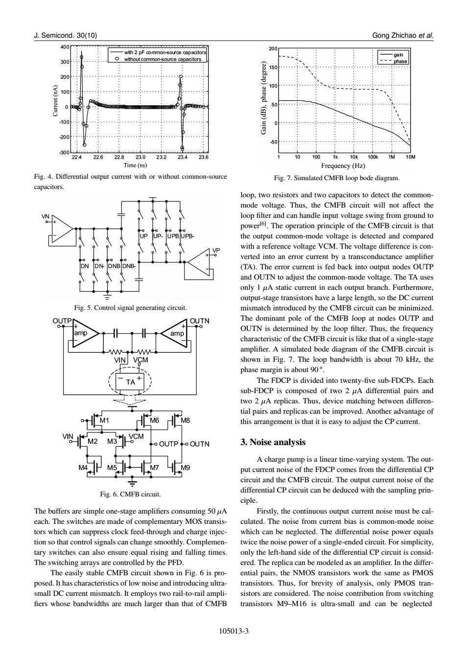
J.Semicond.30(10) Gong Zhichao et al. 400T 200 with 2 pF common-souroe capacitors gain 300 without common-source capacitors 150 ....... ---phase 200 100 100 0 50 -100 200 50 300. 224 22.6 22.823.023.223.4 23.6 1 10 1001k10k100k1M10M Time(ns) Frequency (Hz) Fig.4.Differential output current with or without common-source Fig.7.Simulated CMFB loop bode diagram. capacitors. loop,two resistors and two capacitors to detect the common- mode voltage.Thus,the CMFB circuit will not affect the loop filter and can handle input voltage swing from ground to powerl6).The operation principle of the CMFB circuit is that the output common-mode voltage is detected and compared with a reference voltage VCM.The voltage difference is con- verted into an error current by a transconductance amplifier N DN DNBDNB (TA).The error current is fed back into output nodes OUTP and OUTN to adjust the common-mode voltage.The TA uses only 1 LA static current in each output branch.Furthermore, output-stage transistors have a large length,so the DC current Fig.5.Control signal generating circuit. mismatch introduced by the CMFB circuit can be minimized. OUTPI OUTN The dominant pole of the CMFB loop at nodes OUTP and OUTN is determined by the loop filter.Thus,the frequency amp amp characteristic of the CMFB circuit is like that of a single-stage amplifier.A simulated bode diagram of the CMFB circuit is VCM shown in Fig.7.The loop bandwidth is about 70 kHz,the phase margin is about 90. The FDCP is divided into twenty-five sub-FDCPs.Each sub-FDCP is composed of two 2 uA differential pairs and two 2 uA replicas.Thus,device matching between differen- tial pairs and replicas can be improved.Another advantage of this arrangement is that it is easy to adjust the CP current. VCM M3 OUTN 3.Noise analysis A charge pump is a linear time-varying system.The out- M M7 9 put current noise of the FDCP comes from the differential CP circuit and the CMFB circuit.The output current noise of the Fig.6.CMFB circuit. differential CP circuit can be deduced with the sampling prin- ciple. The buffers are simple one-stage amplifiers consuming 50 uA Firstly,the continuous output current noise must be cal- each.The switches are made of complementary MOS transis- culated.The noise from current bias is common-mode noise tors which can suppress clock feed-through and charge injec- which can be neglected.The differential noise power equals tion so that control signals can change smoothly.Complemen- twice the noise power of a single-ended circuit.For simplicity, tary switches can also ensure equal rising and falling times. only the left-hand side of the differential CP circuit is consid- The switching arrays are controlled by the PFD. ered.The replica can be modeled as an amplifier.In the differ- The easily stable CMFB circuit shown in Fig.6 is pro- ential pairs,the NMOS transistors work the same as PMOS posed.It has characteristics of low noise and introducing ultra- transistors.Thus,for brevity of analysis,only PMOS tran- small DC current mismatch.It employs two rail-to-rail ampli- sistors are considered.The noise contribution from switching fiers whose bandwidths are much larger than that of CMFB transistors M9-M16 is ultra-small and can be neglected 105013-3J. Semicond. 30(10) Gong Zhichao et al. Fig. 4. Differential output current with or without common-source capacitors. Fig. 5. Control signal generating circuit. Fig. 6. CMFB circuit. The buffers are simple one-stage amplifiers consuming 50 µA each. The switches are made of complementary MOS transistors which can suppress clock feed-through and charge injection so that control signals can change smoothly. Complementary switches can also ensure equal rising and falling times. The switching arrays are controlled by the PFD. The easily stable CMFB circuit shown in Fig. 6 is proposed. It has characteristics of low noise and introducing ultrasmall DC current mismatch. It employs two rail-to-rail ampli- fiers whose bandwidths are much larger than that of CMFB Fig. 7. Simulated CMFB loop bode diagram. loop, two resistors and two capacitors to detect the commonmode voltage. Thus, the CMFB circuit will not affect the loop filter and can handle input voltage swing from ground to power[6]. The operation principle of the CMFB circuit is that the output common-mode voltage is detected and compared with a reference voltage VCM. The voltage difference is converted into an error current by a transconductance amplifier (TA). The error current is fed back into output nodes OUTP and OUTN to adjust the common-mode voltage. The TA uses only 1 µA static current in each output branch. Furthermore, output-stage transistors have a large length, so the DC current mismatch introduced by the CMFB circuit can be minimized. The dominant pole of the CMFB loop at nodes OUTP and OUTN is determined by the loop filter. Thus, the frequency characteristic of the CMFB circuit is like that of a single-stage amplifier. A simulated bode diagram of the CMFB circuit is shown in Fig. 7. The loop bandwidth is about 70 kHz, the phase margin is about 90 ◦ . The FDCP is divided into twenty-five sub-FDCPs. Each sub-FDCP is composed of two 2 µA differential pairs and two 2 µA replicas. Thus, device matching between differential pairs and replicas can be improved. Another advantage of this arrangement is that it is easy to adjust the CP current. 3. Noise analysis A charge pump is a linear time-varying system. The output current noise of the FDCP comes from the differential CP circuit and the CMFB circuit. The output current noise of the differential CP circuit can be deduced with the sampling principle. Firstly, the continuous output current noise must be calculated. The noise from current bias is common-mode noise which can be neglected. The differential noise power equals twice the noise power of a single-ended circuit. For simplicity, only the left-hand side of the differential CP circuit is considered. The replica can be modeled as an amplifier. In the differential pairs, the NMOS transistors work the same as PMOS transistors. Thus, for brevity of analysis, only PMOS transistors are considered. The noise contribution from switching transistors M9–M16 is ultra-small and can be neglected 105013-3