正在加载图片...
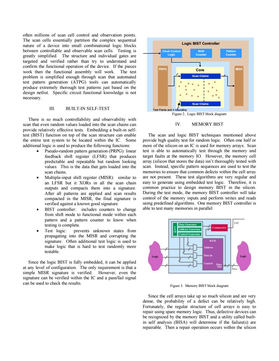
often millions of scan cell control and observation points. The scan cells essentially partition the complex sequential nature of a device into small combinational logic blocks Logic BIST Controller between controllable and observable scan cells.Testing is Clock Control Shift Pattern greatly simplified.The structure and individual gates are Logic Counter Counter targeted and verified rather than try to understand and confirm the functional operation of the device.If the pieces PRPG work then the functional assembly will work.The test Core MISR problem is simplified enough through scan that automated Scan Chains test pattern generation (ATPG)tools can automatically produce extremely thorough test patterns just based on the design netlist.Specific circuit functional knowledge is not necessary. Scan Chains Ⅲ. BUILT-IN SELF-TEST Test Points and X-bounding Figure 2.Logic BIST block diagram There is so much controllability and observability with scan that even random values loaded into the scan chains can IV. MEMORY BIST provide relatively effective tests.Embedding a built-in self- test (BIST)function on top of the scan structure can enable The scan and logic BIST techniques mentioned above the entire test system to be located within the IC.Some provide high quality test for random logic.Often one half or additional logic is used to produce the following functions: more of the silicon on an IC is used for memory arrays.Scan Pseudo-random pattern generation(PRPG):linear test is able to automatically test through the memory and feedback shift register (LFSR)that produces target faults at the memory IO.However,the memory cell predictable and repeatable but random looking array(silicon that stores the data)isn't thoroughly tested with values.This is the data that gets loaded into the scan.Instead,specific pattern sequences are used to test the scan chains. memories to ensure that common defects within the cell array Multiple-input shift register (MISR):similar to are not present.These test algorithms are very regular and an LFSR but it XORs in all the scan chain easy to generate using embedded test logic.Therefore,it is outputs and compacts them into a signature. common practice to design memory BIST in the silicon. After all patterns are applied and scan results During the test mode,the memory BIST controller will take compacted in the MISR,the final signature is control of the memory inputs and perform writes and reads verified against a known good signature. using predefined algorithms.One memory BIST controller is BIST controller:includes counters to change able to test many memories in parallel. from shift mode to functional mode within each pattern and a pattern counter to know when testing is complete. Test logic:prevents unknown states from propagating into the MISR and corrupting the signature.Often additional test logic is used to RAN make logic that is hard to test randomly more testable. Since the logic BIST is fully embedded,it can be applied at any level of configuration.The only requirement is that a simple MISR signature is verified.However,even the signature can be verified within the IC and a pass/fail signal can be used to check the results. Figure 3.Memory BIST block diagram Since the cell arrays take up so much silicon and are very dense,the probability of a defect can be relatively high Fortunately,the regular structure of cell arrays is easy to repair using spare memory logic.Thus,defective devices can be recognized by the memory BIST and a utility called built- in self analysis(BISA)will determine if the failure(s)are repairable.Then a repair operation occurs within the siliconoften millions of scan cell control and observation points. The scan cells essentially partition the complex sequential nature of a device into small combinational logic blocks between controllable and observable scan cells. Testing is greatly simplified. The structure and individual gates are targeted and verified rather than try to understand and confirm the functional operation of the device. If the pieces work then the functional assembly will work. The test problem is simplified enough through scan that automated test pattern generation (ATPG) tools can automatically produce extremely thorough test patterns just based on the design netlist. Specific circuit functional knowledge is not necessary. III. BUILT-IN SELF-TEST There is so much controllability and observability with scan that even random values loaded into the scan chains can provide relatively effective tests. Embedding a built-in selftest (BIST) function on top of the scan structure can enable the entire test system to be located within the IC. Some additional logic is used to produce the following functions: • Pseudo-random pattern generation (PRPG): linear feedback shift register (LFSR) that produces predictable and repeatable but random looking values. This is the data that gets loaded into the scan chains. • Multiple-input shift register (MISR): similar to an LFSR but it XORs in all the scan chain outputs and compacts them into a signature. After all patterns are applied and scan results compacted in the MISR, the final signature is verified against a known good signature. • BIST controller: includes counters to change from shift mode to functional mode within each pattern and a pattern counter to know when testing is complete. • Test logic: prevents unknown states from propagating into the MISR and corrupting the signature. Often additional test logic is used to make logic that is hard to test randomly more testable. Since the logic BIST is fully embedded, it can be applied at any level of configuration. The only requirement is that a simple MISR signature is verified. However, even the signature can be verified within the IC and a pass/fail signal can be used to check the results. Figure 2. Logic BIST block diagram IV. MEMORY BIST The scan and logic BIST techniques mentioned above provide high quality test for random logic. Often one half or more of the silicon on an IC is used for memory arrays. Scan test is able to automatically test through the memory and target faults at the memory IO. However, the memory cell array (silicon that stores the data) isn’t thoroughly tested with scan. Instead, specific pattern sequences are used to test the memories to ensure that common defects within the cell array are not present. These test algorithms are very regular and easy to generate using embedded test logic. Therefore, it is common practice to design memory BIST in the silicon. During the test mode, the memory BIST controller will take control of the memory inputs and perform writes and reads using predefined algorithms. One memory BIST controller is able to test many memories in parallel. Figure 3. Memory BIST block diagram Since the cell arrays take up so much silicon and are very dense, the probability of a defect can be relatively high. Fortunately, the regular structure of cell arrays is easy to repair using spare memory logic. Thus, defective devices can be recognized by the memory BIST and a utility called builtin self analysis (BISA) will determine if the failure(s) are repairable. Then a repair operation occurs within the silicon Logic BIST Controller Core PRPG Test Points and X-bounding Scan Chains Scan Chains Clock Control Logic MISR Shift Counter Pattern Counter