正在加载图片...
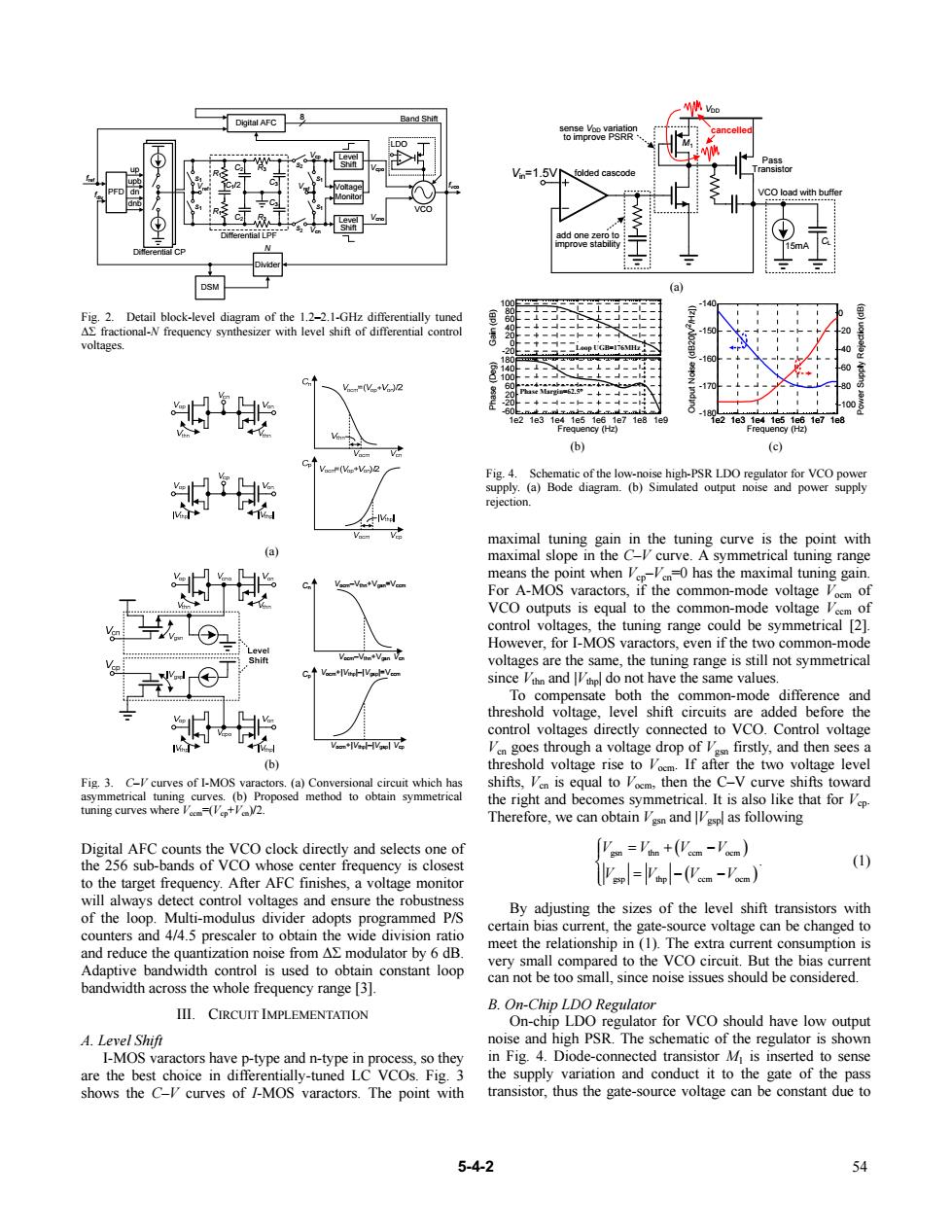
Digital AFC Band Shif V=1.5V O load with buff DSM 00 Fig.2.Detail block-level diagram of the 1.2-2.1-GHz differentially tuned AE fractional-N frequency synthesizer with level shift of differential control voltages. Vi(Vp+Vo)2 60 楼 60 e2 V (b) (c) VF(Vis+V)2 Fig.4.Schematic of the low-noise high-PSR LDO regulator for VCO power supply.(a)Bode diagram.(b)Simulated output noise and power supply rejection. maximal tuning gain in the tuning curve is the point with (a) maximal slope in the C-Vcurve.A symmetrical tuning range 并楼 means the point when Vep-Vn-0 has the maximal tuning gain. T-VE+ For A-MOS varactors,if the common-mode voltage Vocm of VCO outputs is equal to the common-mode voltage Veem of control voltages,the tuning range could be symmetrical [2]. However,for I-MOS varactors,even if the two common-mode Veon-VintVan Ve voltages are the same,the tuning range is still not symmetrical C↑Van+Vinch-lVapl-V.on since Ihn and IIthpl do not have the same values. To compensate both the common-mode difference and threshold voltage,level shift circuits are added before the control voltages directly connected to VCO.Control voltage IVsl-IVael Ve Ven goes through a voltage drop of Vasn firstly,and then sees a (b) threshold voltage rise to Vocm.If after the two voltage level Fig.3.C-V curves of I-MOS varactors.(a)Conversional circuit which ha shifts,Ven is equal to Vocm,then the C-V curve shifts toward asymmetrical tuning curves.(b)Proposed method to obtain symmetrical the right and becomes symmetrical.It is also like that for Vep. tuning curves where V2. Therefore,we can obtain Vasn and IVgsp as following Digital AFC counts the VCO clock directly and selects one of f'n=a+('.m-'.em) the 256 sub-bands of VCO whose center frequency is closest (1) to the target frequency.After AFC finishes,a voltage monitor Vpp=Vop-(Vscm-Vacm) will always detect control voltages and ensure the robustness of the loop.Multi-modulus divider adopts programmed P/S By adjusting the sizes of the level shift transistors with counters and 4/4.5 prescaler to obtain the wide division ratio certain bias current,the gate-source voltage can be changed to meet the relationship in (1).The extra current consumption is and reduce the quantization noise from A modulator by 6 dB. Adaptive bandwidth control is used to obtain constant loop very small compared to the VCO circuit.But the bias current can not be too small,since noise issues should be considered. bandwidth across the whole frequency range [3]. III.CIRCUIT IMPLEMENTATION B.On-Chip LDO Regulator On-chip LDO regulator for VCO should have low output A.Level Shift noise and high PSR.The schematic of the regulator is shown I-MOS varactors have p-type and n-type in process,so they in Fig.4.Diode-connected transistor M is inserted to sense are the best choice in differentially-tuned LC VCOs.Fig.3 the supply variation and conduct it to the gate of the pass shows the C-V curves of I-MOS varactors.The point with transistor,thus the gate-source voltage can be constant due to 5-4-2 54Digital AFC counts the VCO clock directly and selects one of the 256 sub-bands of VCO whose center frequency is closest to the target frequency. After AFC finishes, a voltage monitor will always detect control voltages and ensure the robustness of the loop. Multi-modulus divider adopts programmed P/S counters and 4/4.5 prescaler to obtain the wide division ratio and reduce the quantization noise from ΔΣ modulator by 6 dB. Adaptive bandwidth control is used to obtain constant loop bandwidth across the whole frequency range [3]. III. CIRCUIT IMPLEMENTATION A. Level Shift I-MOS varactors have p-type and n-type in process, so they are the best choice in differentially-tuned LC VCOs. Fig. 3 shows the C–V curves of I-MOS varactors. The point with maximal tuning gain in the tuning curve is the point with maximal slope in the C–V curve. A symmetrical tuning range means the point when Vcp–Vcn=0 has the maximal tuning gain. For A-MOS varactors, if the common-mode voltage Vocm of VCO outputs is equal to the common-mode voltage Vccm of control voltages, the tuning range could be symmetrical [2]. However, for I-MOS varactors, even if the two common-mode voltages are the same, the tuning range is still not symmetrical since Vthn and |Vthp| do not have the same values. To compensate both the common-mode difference and threshold voltage, level shift circuits are added before the control voltages directly connected to VCO. Control voltage Vcn goes through a voltage drop of Vgsn firstly, and then sees a threshold voltage rise to Vocm. If after the two voltage level shifts, Vcn is equal to Vocm, then the C–V curve shifts toward the right and becomes symmetrical. It is also like that for Vcp. Therefore, we can obtain Vgsn and |Vgsp| as following ( ) ( ) gsn thn ccm ocm gsp thp ccm ocm . ⎧ =+ − ⎪ ⎨ =− − ⎪⎩ VV VV V V VV (1) By adjusting the sizes of the level shift transistors with certain bias current, the gate-source voltage can be changed to meet the relationship in (1). The extra current consumption is very small compared to the VCO circuit. But the bias current can not be too small, since noise issues should be considered. B. On-Chip LDO Regulator On-chip LDO regulator for VCO should have low output noise and high PSR. The schematic of the regulator is shown in Fig. 4. Diode-connected transistor M1 is inserted to sense the supply variation and conduct it to the gate of the pass transistor, thus the gate-source voltage can be constant due to Differential LPF PFD Digital AFC fref R1 R1 C1/2 C2 C2 R3 R3 C3 C3 Vref s1 s1 s2 s2 Differential CP up upb dn dnb Level Shift Vref s1 s1 Vcp Vcn Vcpo Vcno Divider DSM N fvco 8 Band Shift VCO LDO fdiv Voltage Monitor Level Shift Fig. 2. Detail block-level diagram of the 1.2–2.1-GHz differentially tuned ΔΣ fractional-N frequency synthesizer with level shift of differential control voltages. (a) Vcn Cn Vocm–Vthn+Vgsn Vcp Cp Vocm+|Vthp|–|Vgsp| Vocm–Vthn+Vgsn=Vccm Vocm+|Vthp|–|Vgsp|=Vccm (b) Fig. 3. C–V curves of I-MOS varactors. (a) Conversional circuit which has asymmetrical tuning curves. (b) Proposed method to obtain symmetrical tuning curves where Vccm=(Vcp+Vcn)/2. Vin=1.5V add one zero to improve stability sense VDD variation to improve PSRR Pass Transistor folded cascode CL 15mA VDD cancelled VCO load with buffer M1 (a) -20 0 20 40 60 80 100 Gain (dB) 1e2 1e3 1e4 1e5 1e6 1e7 1e8 1e9 -60 -20 20 60 100 140 180 Frequency (Hz) Phase (Deg) Loop UGB=176MHz Phase Margin=62.5° (b) 1e2 1e3 1e4 1e5 1e6 1e7 1e8 -180 -170 -160 -150 -140 Frequency (Hz) Output Noise (dB20[V2/Hz]) 1e2 1e3 1e4 1e5 1e6 1e7 1e8 -100 -80 -60 -40 -20 0 Power Supply Rejection (dB) (c) Fig. 4. Schematic of the low-noise high-PSR LDO regulator for VCO power supply. (a) Bode diagram. (b) Simulated output noise and power supply rejection. 5-4-2 54