正在加载图片...
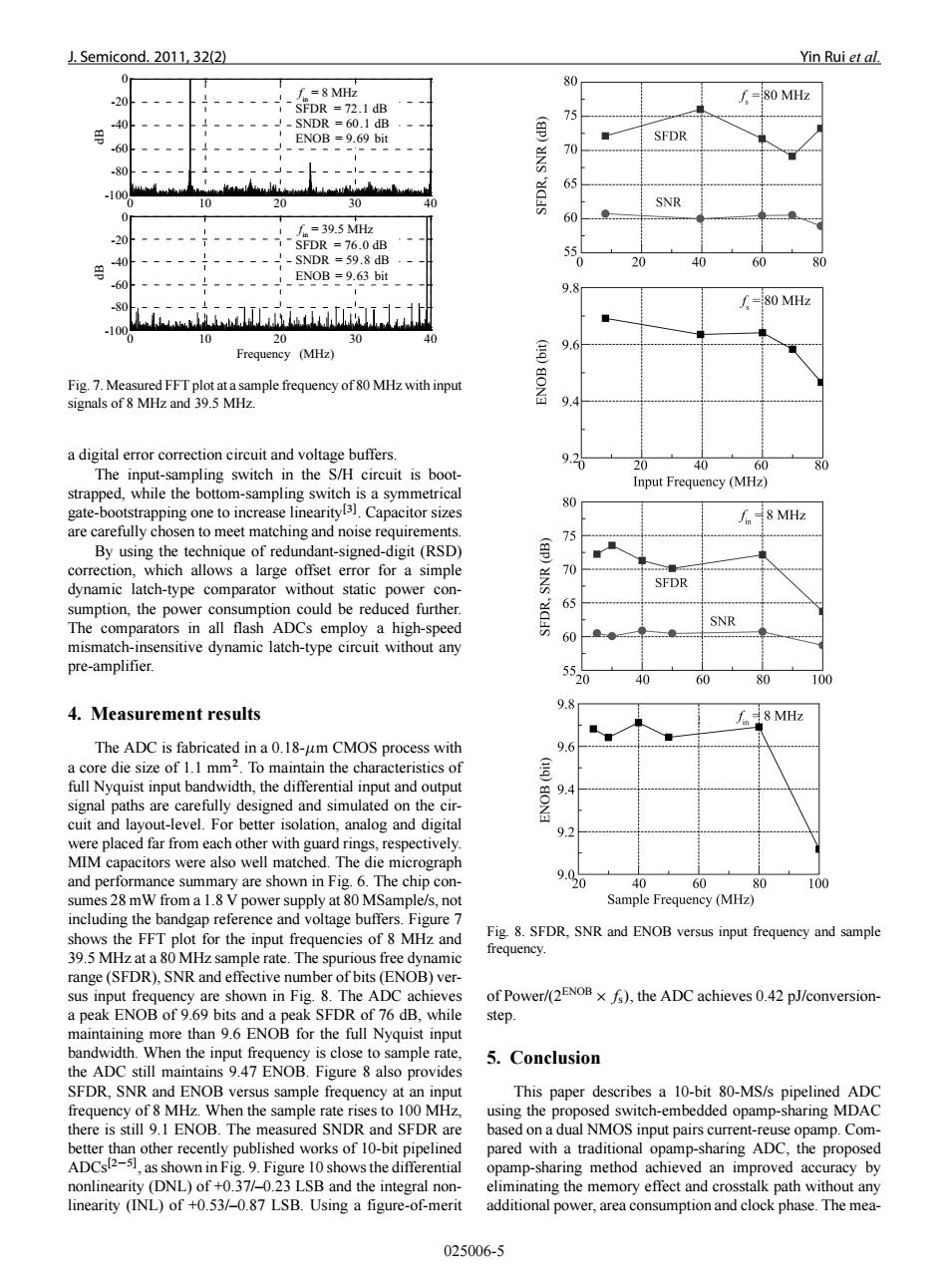
.Semicond.2011,32(2) Yin Rui et al. 0 80 =8 MHz -20 =80 MHz SFDR =72.1 dB 40/ SNDR =60.1 dB 75 ENOB =9.69 bit SFDR -60 1 70 -80 ---1------ 65 -100 0 10 20 30 40 SNR 60 -20 =39.5 MHz -----7 ------sFDR=76.0dB 55 40 --------- -SNDR =59.8 dB 20 40 60 80 60-----}----- 1 ENOB =9.63 bit 9.8 -80 80 MHz 1000 FKMm 10 20 30 40 (q) 9.6 Frequency (MHz) Fig.7.Measured FFT plot at a sample frequency of 80 MHz with input signals of 8 MHz and 39.5 MHz. a digital error correction circuit and voltage buffers. 20 40 80 The input-sampling switch in the S/H circuit is boot- 60 Input Frequency (MHz) strapped,while the bottom-sampling switch is a symmetrical gate-bootstrapping one to increase linearityl3).Capacitor sizes 80 f8 MHz are carefully chosen to meet matching and noise requirements. 75 By using the technique of redundant-signed-digit(RSD) e ◆ correction,which allows a large offset error for a simple 0 dynamic latch-type comparator without static power con- SFDR sumption,the power consumption could be reduced further. 65 The comparators in all flash ADCs employ a high-speed SNR 60 mismatch-insensitive dynamic latch-type circuit without any pre-amplifier. 55 0 40 60 80 100 9.8 4.Measurement results 8 MHz The ADC is fabricated in a 0.18-um CMOS process with 9.6H a core die size of 1.1 mm2.To maintain the characteristics of 邑 full Nyquist input bandwidth,the differential input and output 9.4 signal paths are carefully designed and simulated on the cir- cuit and layout-level.For better isolation,analog and digital 9.2 were placed far from each other with guard rings,respectively. MIM capacitors were also well matched.The die micrograph and performance summary are shown in Fig.6.The chip con- 900 40 60 80 100 sumes 28 mW from a 1.8 V power supply at 80 MSample/s,not Sample Frequency (MHz) including the bandgap reference and voltage buffers.Figure 7 shows the FFT plot for the input frequencies of 8 MHz and Fig.8.SFDR,SNR and ENOB versus input frequency and sample 39.5 MHz at a 80 MHz sample rate.The spurious free dynamic frequency range(SFDR),SNR and effective number of bits(ENOB)ver- sus input frequency are shown in Fig.8.The ADC achieves of Power/(2ENOB x fs),the ADC achieves 0.42 pJ/conversion- a peak ENOB of 9.69 bits and a peak SFDR of 76 dB,while step maintaining more than 9.6 ENOB for the full Nyquist input bandwidth.When the input frequency is close to sample rate, 5.Conclusion the ADC still maintains 9.47 ENOB.Figure 8 also provides SFDR,SNR and ENOB versus sample frequency at an input This paper describes a 10-bit 80-MS/s pipelined ADC frequency of 8 MHz.When the sample rate rises to 100 MHz, using the proposed switch-embedded opamp-sharing MDAC there is still 9.1 ENOB.The measured SNDR and SFDR are based on a dual NMOS input pairs current-reuse opamp.Com- better than other recently published works of 10-bit pipelined pared with a traditional opamp-sharing ADC,the proposed ADCs2-51,as shown in Fig.9.Figure 10 shows the differential opamp-sharing method achieved an improved accuracy by nonlinearity (DNL)of +0.37/-0.23 LSB and the integral non- eliminating the memory effect and crosstalk path without any linearity (INL)of +0.53/-0.87 LSB.Using a figure-of-merit additional power,area consumption and clock phase.The mea- 025006-5J. Semicond. 2011, 32(2) Yin Rui et al. 0 10 20 30 40 -100 -80 -60 -40 -20 0 0 10 20 30 40 -100 -40 -20 0 -80 -60 dB dB Frequency (MHz) f in = 8 MHz SFDR = 72.1 dB SNDR = 60.1 dB ENOB = 9.69 bit f in = 39.5 MHz SFDR = 76.0 dB SNDR = 59.8 dB ENOB = 9.63 bit Fig. 7. Measured FFT plot at a sample frequency of 80 MHz with input signals of 8 MHz and 39.5 MHz. a digital error correction circuit and voltage buffers. The input-sampling switch in the S/H circuit is bootstrapped, while the bottom-sampling switch is a symmetrical gate-bootstrapping one to increase linearityŒ3. Capacitor sizes are carefully chosen to meet matching and noise requirements. By using the technique of redundant-signed-digit (RSD) correction, which allows a large offset error for a simple dynamic latch-type comparator without static power consumption, the power consumption could be reduced further. The comparators in all flash ADCs employ a high-speed mismatch-insensitive dynamic latch-type circuit without any pre-amplifier. 4. Measurement results The ADC is fabricated in a 0.18-m CMOS process with a core die size of 1.1 mm2 . To maintain the characteristics of full Nyquist input bandwidth, the differential input and output signal paths are carefully designed and simulated on the circuit and layout-level. For better isolation, analog and digital were placed far from each other with guard rings, respectively. MIM capacitors were also well matched. The die micrograph and performance summary are shown in Fig. 6. The chip consumes 28 mW from a 1.8 V power supply at 80 MSample/s, not including the bandgap reference and voltage buffers. Figure 7 shows the FFT plot for the input frequencies of 8 MHz and 39.5 MHz at a 80 MHz sample rate. The spurious free dynamic range (SFDR), SNR and effective number of bits (ENOB) versus input frequency are shown in Fig. 8. The ADC achieves a peak ENOB of 9.69 bits and a peak SFDR of 76 dB, while maintaining more than 9.6 ENOB for the full Nyquist input bandwidth. When the input frequency is close to sample rate, the ADC still maintains 9.47 ENOB. Figure 8 also provides SFDR, SNR and ENOB versus sample frequency at an input frequency of 8 MHz. When the sample rate rises to 100 MHz, there is still 9.1 ENOB. The measured SNDR and SFDR are better than other recently published works of 10-bit pipelined ADCsŒ25, as shown in Fig. 9. Figure 10 shows the differential nonlinearity (DNL) of +0.37/–0.23 LSB and the integral nonlinearity (INL) of +0.53/–0.87 LSB. Using a figure-of-merit Fig. 8. SFDR, SNR and ENOB versus input frequency and sample frequency. of Power/(2ENOB fs/, the ADC achieves 0.42 pJ/conversionstep. 5. Conclusion This paper describes a 10-bit 80-MS/s pipelined ADC using the proposed switch-embedded opamp-sharing MDAC based on a dual NMOS input pairs current-reuse opamp. Compared with a traditional opamp-sharing ADC, the proposed opamp-sharing method achieved an improved accuracy by eliminating the memory effect and crosstalk path without any additional power, area consumption and clock phase. The mea- 025006-5�