正在加载图片...

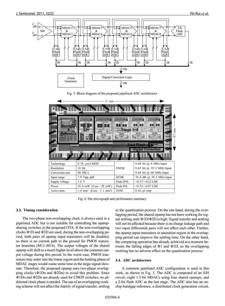
1.Semicond.2011,32(2) Yin Rui et al. MDAC3 MDAC5 MDAC7 2-b S/H Flash MDAC2 MDAC4 MDAC6 MDAC8 ADC ADC h 2b /18b Clock Digital Correction Logic Generator 10 Fig.5.Block diagram of the proposed pipelined ADC architecture. mm igital Correction Technology 0.18-um CMOS 9.69 bit 8 MHz Input Resolution 10 bit ENOB 9.63 bit 39.5 MHz Input Conversion rate 80 MS/s 9.64 bit 60 MHz Input Input range 1.6 Vpp,diff SFDR 76.0 dB 39.5 MHz Input Supply voltage 1.8V Peak DNL +0.37/-0.23LSB Power 32.4 mW (Core:28 mW) Peak INL +0.53/-0.87LSB Active area 1.4 mm2 (Core:1.1 mm2) FOM 0.42 pJ/step Fig.6.Die micrograph and performance summary. 3.3.Timing consideration or the quantization process.On the one hand,during the over- lapping period,the shared opamp has not been working for sig- The two-phase non-overlapping clock is always used in a nal settling until 1D/2D is high.Signal transfer and settling pipelined ADC but is not suitable for controlling the opamp- will not be affected because there is no charge leakage path and sharing switches in the proposed OTA.If the non-overlapping two input differential pairs will not affect each other.Further. clocks 1D and 2D are used,during the non-overlapping pe- the opamp input transistors in saturation region in the overlap- riod,both pairs of opamp input transistors will be disabled, ping period can improve the settling time.On the other hand. so there is no current path to the ground for PMOS transis- the comparing operation has already achieved at a moment be- tor branches (M11-M14).The output voltages of the shared tween the falling edges of I and ID,so the overlapping opamp will shift to a much higher level above the common out- working has no adverse effect on the quantization process. put voltage during this period.In the worst case,PMOS tran- sistors may enter into the linear region and the holding phase of 3.4.ADC architecture MDAC stages would waste some time in the large-signal slew- rate.Therefore,the proposed opamp uses two-phase overlap- A common pipelined ADC configuration is used in this ping clocks (1Dn and 2Dn)to avoid this problem.Since work,as shown in Fig.5.The ADC is composed of an S/H IDn and 2Dn are already used for CMOS switches,no ad- circuit,eight 1.5-bit MDACs using four shared opamps,and ditional clock phase is needed.The use of an overlapping work- a 2-bit flash ADC as the last stage.The ADC also has an on- ing scheme will not affect the fidelity of signal transfer,settling chip bandgap reference,a distributed clock generation circuit, 025006-4J. Semicond. 2011, 32(2) Yin Rui et al. Clock Digital Correction Logic Generator Vinp Vinn 18b 10b MDAC1 & MDAC2 S/H 2b 2-b Flash ADC 1.5-b Flash ADC 2b 1.5-b Flash ADC 2b MDAC3 & MDAC4 1.5-b Flash ADC 2b Flash ADC 2b MDAC5 & MDAC6 1.5-b 1.5-b Flash ADC 2b 1.5-b Flash ADC 2b MDAC7 & MDAC8 1.5-b Flash ADC 2b 1.5-b Flash ADC 2b Fig. 5. Block diagram of the proposed pipelined ADC architecture. Fig. 6. Die micrograph and performance summary. 3.3. Timing consideration The two-phase non-overlapping clock is always used in a pipelined ADC but is not suitable for controlling the opampsharing switches in the proposed OTA. If the non-overlapping clocks ˆ1D and ˆ2D are used, during the non-overlapping period, both pairs of opamp input transistors will be disabled, so there is no current path to the ground for PMOS transistor branches (M11–M14). The output voltages of the shared opamp will shift to a much higher level above the common output voltage during this period. In the worst case, PMOS transistors may enter into the linear region and the holding phase of MDAC stages would waste some time in the large-signal slewrate. Therefore, the proposed opamp uses two-phase overlapping clocks (ˆ1Dn and ˆ2Dn) to avoid this problem. Since ˆ1Dn and ˆ2Dn are already used for CMOS switches, no additional clock phase is needed. The use of an overlapping working scheme will not affect the fidelity of signal transfer, settling or the quantization process. On the one hand, during the overlapping period, the shared opamp has not been working for signal settling until ˆ1D/ˆ2D is high. Signal transfer and settling will not be affected because there is no charge leakage path and two input differential pairs will not affect each other. Further, the opamp input transistors in saturation region in the overlapping period can improve the settling time. On the other hand, the comparing operation has already achieved at a moment between the falling edges of ˆ1 and ˆ1D, so the overlapping working has no adverse effect on the quantization process. 3.4. ADC architecture A common pipelined ADC configuration is used in this work, as shown in Fig. 5. The ADC is composed of an S/H circuit, eight 1.5-bit MDACs using four shared opamps, and a 2-bit flash ADC as the last stage. The ADC also has an onchip bandgap reference, a distributed clock generation circuit, 025006-4