正在加载图片...
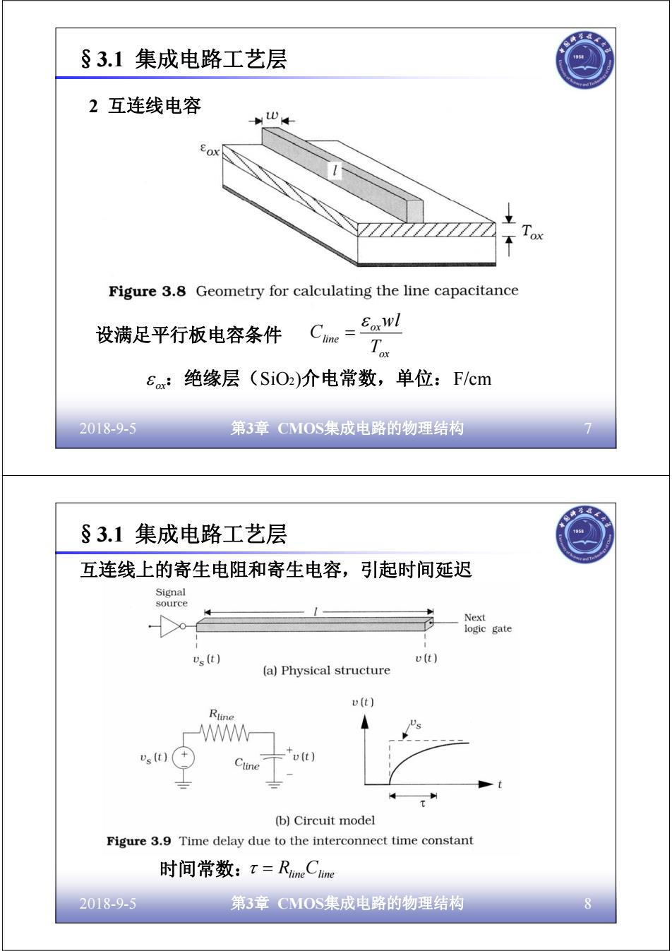
§3.1集成电路工艺层 2互连线电容 EOX o Figure 3.8 Geometry for calculating the line capacitance 设满足平行板电容条件 Ciae-£aswl &:绝缘层(SiO2)介电常数,单位:F/cm 2018-9-5 第3章CMOS集成电路的物理结构 §3.1集成电路工艺层 互连线上的寄生电阻和寄生电容,引起时间延迟 Signal source Next ● logic gate 's(t) v(t) (a)Physical structure v(t) vs(t) "v(t) (b)Circuit model Figure 3.9 Time delay due to the interconnect time constant 时间常数:T=RimneCuine 2018-9-5 第3章CMOS集成电路的物理结构 82018-9-5 第3章 CMOS集成电路的物理结构 7 §3.1 集成电路工艺层 2 互连线电容 设满足平行板电容条件 ox ox line T wl C ε = ε ox:绝缘层(SiO2)介电常数,单位:F/cm 2018-9-5 第3章 CMOS集成电路的物理结构 8 §3.1 集成电路工艺层 互连线上的寄生电阻和寄生电容,引起时间延迟 时间常数: = RlineCline τ