正在加载图片...
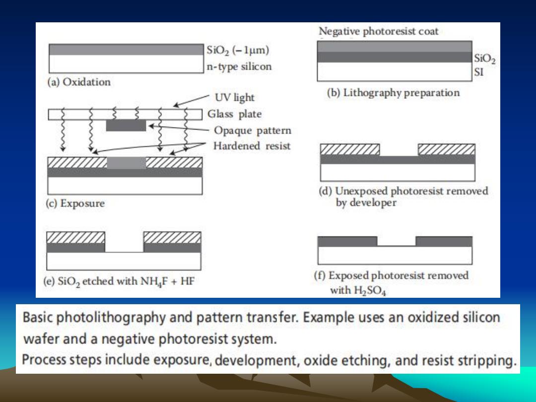
Negative photoresist coat Si02(-1μm) SiO2 n-type silicon SI (a)Oxidation UV light (b)Lithography preparation Glass plate Opaque pattern Hardened resist (d)Unexposed photoresist removed (c)Exposure by developer (e)SiO2 etched with NH F+HF (f)Exposed photoresist removed with H2SO4 Basic photolithography and pattern transfer.Example uses an oxidized silicon wafer and a negative photoresist system. Process steps include exposure,development,oxide etching,and resist stripping