正在加载图片...
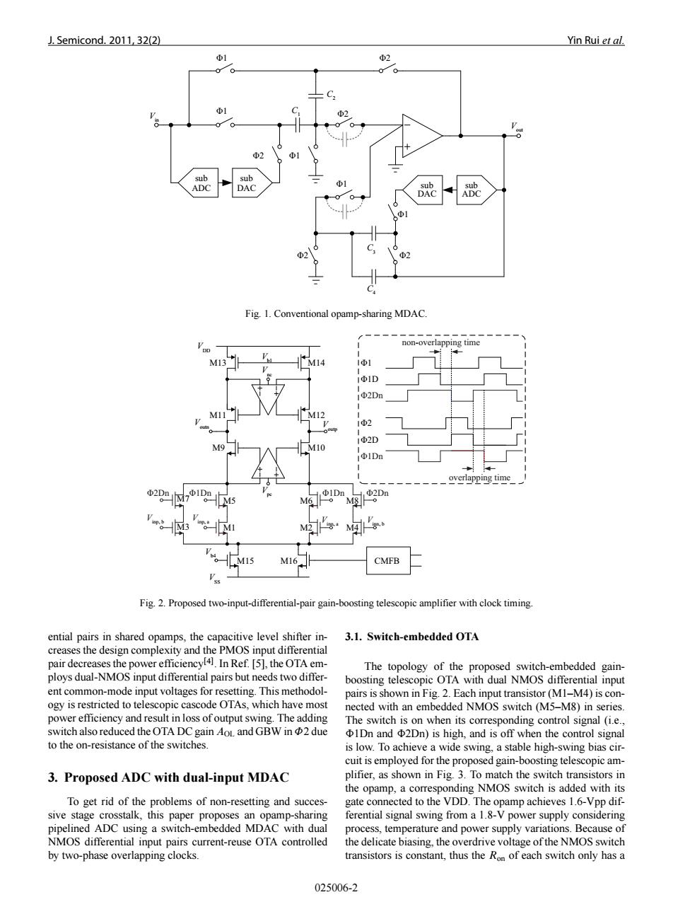
1.Semicond.2011,32(2) Yin Rui et al. Φ1 2 Φ1 2 sub sub ADC DAC sub sub DAC Fig.1.Conventional opamp-sharing MDAC. non-overlapping time M13 1Φ1 iΦ1D 1D2 2D iDn overlapping time b2D加 IDn 2Dn M6 M& M2 M15 M16 CMFB Fig.2.Proposed two-input-differential-pair gain-boosting telescopic amplifier with clock timing. ential pairs in shared opamps,the capacitive level shifter in- 3.1.Switch-embedded OTA creases the design complexity and the PMOS input differential pair decreases the power efficiency[41.In Ref.[5],the OTA em- The topology of the proposed switch-embedded gain- ploys dual-NMOS input differential pairs but needs two differ- boosting telescopic OTA with dual NMOS differential input ent common-mode input voltages for resetting.This methodol- pairs is shown in Fig.2.Each input transistor(M1-M4)is con- ogy is restricted to telescopic cascode OTAs,which have most nected with an embedded NMOS switch(M5-M8)in series. power efficiency and result in loss of output swing.The adding The switch is on when its corresponding control signal (i.e. switch also reduced the OTA DC gain AoL and GBW in 2 due IDn and 2Dn)is high,and is off when the control signal to the on-resistance of the switches. is low.To achieve a wide swing,a stable high-swing bias cir- cuit is employed for the proposed gain-boosting telescopic am- 3.Proposed ADC with dual-input MDAC plifier,as shown in Fig.3.To match the switch transistors in the opamp,a corresponding NMOS switch is added with its To get rid of the problems of non-resetting and succes- gate connected to the VDD.The opamp achieves 1.6-Vpp dif- sive stage crosstalk,this paper proposes an opamp-sharing ferential signal swing from a 1.8-V power supply considering pipelined ADC using a switch-embedded MDAC with dual process,temperature and power supply variations.Because of NMOS differential input pairs current-reuse OTA controlled the delicate biasing,the overdrive voltage of the NMOS switch by two-phase overlapping clocks. transistors is constant,thus the Ron of each switch only has a 025006-2J. Semicond. 2011, 32(2) Yin Rui et al. Φ1 Φ2 C4 C1 C3 C2 sub DAC sub ADC Φ1 Φ1 Φ2 Φ1 Φ2 Φ2 sub ADC sub DAC Vout Vin Φ2 Φ1 Fig. 1. Conventional opamp-sharing MDAC. Vb1 Vb4 Vinn, a Vinp, b Vinp, a Vinn, b Φ2Dn Φ1Dn Φ1Dn Φ2Dn M3 M1 M2 M4 M5 M6 M8 M9 M10 M11 M12 M13 M14 M15 M16 CMFB Voutn Voutp Vnc Vpc Φ1 Φ1D Φ1Dn Φ2 Φ2D Φ2Dn overlapping time non-overlapping time VSS VDD M7 Fig. 2. Proposed two-input-differential-pair gain-boosting telescopic amplifier with clock timing. ential pairs in shared opamps, the capacitive level shifter increases the design complexity and the PMOS input differential pair decreases the power efficiencyŒ4. In Ref. [5], the OTA employs dual-NMOS input differential pairs but needs two different common-mode input voltages for resetting. This methodology is restricted to telescopic cascode OTAs, which have most power efficiency and result in loss of output swing. The adding switch also reduced the OTA DC gain AOL and GBW in ˚2 due to the on-resistance of the switches. 3. Proposed ADC with dual-input MDAC To get rid of the problems of non-resetting and successive stage crosstalk, this paper proposes an opamp-sharing pipelined ADC using a switch-embedded MDAC with dual NMOS differential input pairs current-reuse OTA controlled by two-phase overlapping clocks. 3.1. Switch-embedded OTA The topology of the proposed switch-embedded gainboosting telescopic OTA with dual NMOS differential input pairs is shown in Fig. 2. Each input transistor (M1–M4) is connected with an embedded NMOS switch (M5–M8) in series. The switch is on when its corresponding control signal (i.e., ˆ1Dn and ˆ2Dn) is high, and is off when the control signal is low. To achieve a wide swing, a stable high-swing bias circuit is employed for the proposed gain-boosting telescopic amplifier, as shown in Fig. 3. To match the switch transistors in the opamp, a corresponding NMOS switch is added with its gate connected to the VDD. The opamp achieves 1.6-Vpp differential signal swing from a 1.8-V power supply considering process, temperature and power supply variations. Because of the delicate biasing, the overdrive voltage of the NMOS switch transistors is constant, thus the Ron of each switch only has a 025006-2