正在加载图片...
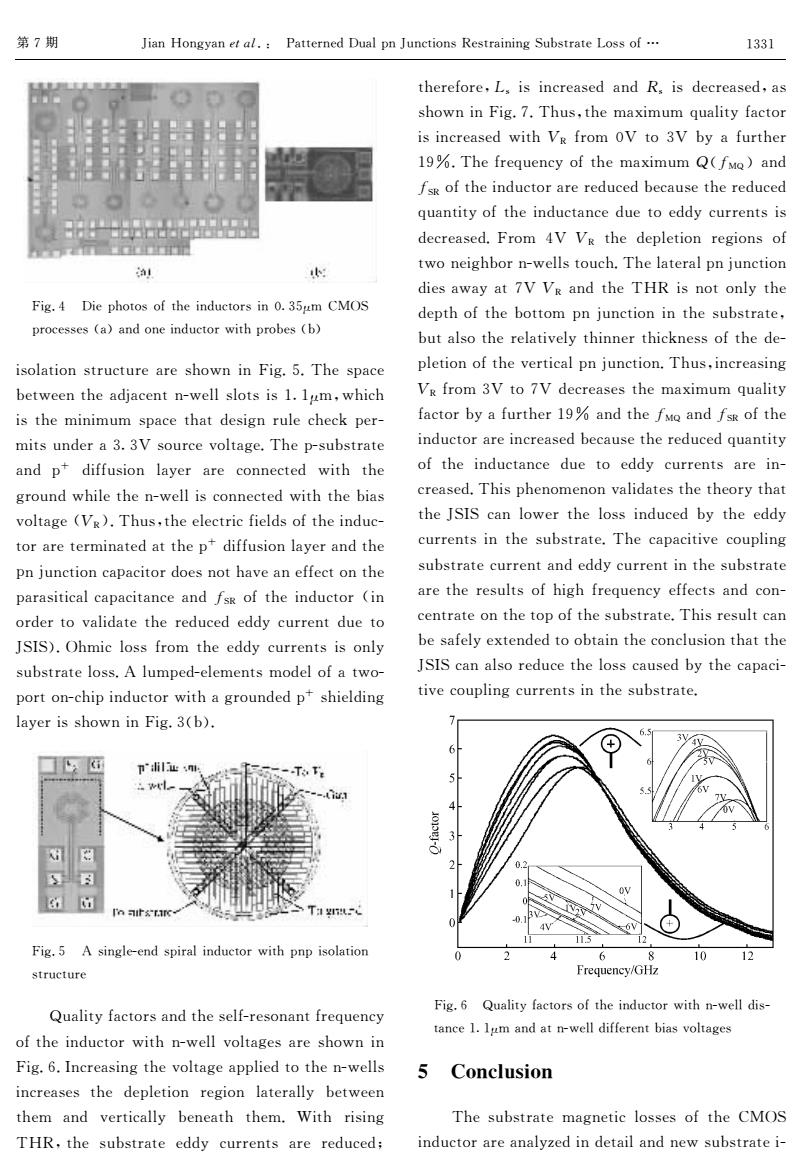
第7期 Jian Hongyan et al.:Patterned Dual pn Junctions Restraining Substrate Loss of... 1331 therefore,L,is increased and R,is decreased,as shown in Fig.7.Thus,the maximum quality factor is increased with Vg from OV to 3V by a further ■ 19%.The frequency of the maximum Q(fMQ)and fsg of the inductor are reduced because the reduced quantity of the inductance due to eddy currents is ■41级服w出■ 。国■ decreased.From 4V Vg the depletion regions of two neighbor n-wells touch.The lateral pn junction AI dies away at 7V Vg and the THR is not only the Fig.4 Die photos of the inductors in 0.35um CMOS depth of the bottom pn junction in the substrate, processes (a)and one inductor with probes (b) but also the relatively thinner thickness of the de- isolation structure are shown in Fig.5.The space pletion of the vertical pn junction.Thus,increasing between the adjacent n-well slots is 1.Ium,which V&from 3V to 7V decreases the maximum quality is the minimum space that design rule check per- factor by a further 19%and the fMo and fsk of the mits under a 3.3V source voltage.The p-substrate inductor are increased because the reduced quantity and p diffusion layer are connected with the of the inductance due to eddy currents are in- ground while the n-well is connected with the bias creased.This phenomenon validates the theory that voltage (VR).Thus,the electric fields of the induc- the JSIS can lower the loss induced by the eddy tor are terminated at the p diffusion layer and the currents in the substrate.The capacitive coupling pn junction capacitor does not have an effect on the substrate current and eddy current in the substrate parasitical capacitance and fsg of the inductor (in are the results of high frequency effects and con- order to validate the reduced eddy current due to centrate on the top of the substrate.This result can JSIS).Ohmic loss from the eddy currents is only be safely extended to obtain the conclusion that the substrate loss.A lumped-elements model of a two- JSIS can also reduce the loss caused by the capaci- port on-chip inductor with a grounded p shielding tive coupling currents in the substrate. layer is shown in Fig.3(b). 3V 4 pi业 T下 -C 8 日 0. OV T15 0.1 4V 11 11.5 12 Fig.5 A single-end spiral inductor with pnp isolation 4 6 8 10 12 structure Frequency/GHz Fig.6 Quality factors of the inductor with n-well dis- Quality factors and the self-resonant frequency tance 1.lum and at n-well different bias voltages of the inductor with n-well voltages are shown in Fig.6.Increasing the voltage applied to the n-wells 5 Conclusion increases the depletion region laterally between them and vertically beneath them.With rising The substrate magnetic losses of the CMOS THR,the substrate eddy currents are reduced; inductor are analyzed in detail and new substrate i-第M期 Y$&)8()36&)*M#8T! +&’’;.);,U2&#")Y2)%’$()7P;7’.&$)$)312G7’.&’;?(77(*" F$3cX U$;"4(’(7(*’4;$),2%’(.7$)W‘ZV!0 5DR1 ".(%;77;7#&$&),();$),2%’(.T$’4".(G;7#G$ $7(#&’$()7’.2%’2.;&.;74(T)$)F$3cVcQ4;7"&%; G;’T;;)’4;&,@&%;)’)[T;##7#(’7$7A‘A!0%T4$%4 $7’4;0$)$0207"&%;’4&’,;7$3).2#;%4;%^";.[ 0$’72),;.&Z‘ZH7(2.%;O(#’&3;cQ4;"[72G7’.&’; &), "k ,$**27$() #&6;. &.; %());%’;, T$’4 ’4; 3.(2),T4$#;’4;)[T;##$7%());%’;,T$’4’4;G$&7 O(#’&3;#\P$cQ427%’4;;#;%’.$%*$;#,7(*’4;$),2%[ ’(.&.;’;.0$)&’;,&’’4;"k ,$**27$()#&6;.&),’4; ")@2)%’$()%&"&%$’(.,(;7)(’4&O;&);**;%’()’4; "&.&7$’$%&#%&"&%$’&)%;&),=1P (*’4;$),2%’(. #$) (.,;.’(O&#$,&’;’4;.;,2%;,;,,6%2..;)’,2;’( Y1J1$cR40$%#(77*.(0’4;;,,6%2..;)’7$7()#6 72G7’.&’;#(77c!#20";,[;#;0;)’70(,;#(*&’T([ "(.’()[%4$"$),2%’(.T$’4&3.(2),;,"k 74$;#,$)3 #&6;.$774(T)$)F$3cZ#G$c F$3cV !7$)3#;[;),7"$.&#$),2%’(.T$’4")"$7(#&’$() 7’.2%’2.; <2&#$’6*&%’(.7&),’4;7;#*[.;7()&)’*.;]2;)%6 (*’4;$),2%’(.T$’4)[T;##O(#’&3;7&.;74(T)$) F$3c_cJ)%.;&7$)3’4;O(#’&3;&""#$;,’(’4;)[T;##7 $)%.;&7;7’4; ,;"#;’$() .;3$()#&’;.&##6 G;’T;;) ’4;0 &), O;.’$%&##6 G;);&’4 ’4;0c>$’4 .$7$)3 Q8P%’4;72G7’.&’;;,,6 %2..;)’7&.;.;,2%;,& ’4;.;*(.;%17$7$)%.;&7;,&),E7$7,;%.;&7;,%&7 74(T)$)F$3cMcQ427%’4;0&/$020]2&#$’6*&%’(. $7$)%.;&7;,T$’4\P *.(0WH’(ZH G6&*2.’4;. ASgcQ4;*.;]2;)%6(*’4;0&/$020,#=D< $&), =1P(*’4;$),2%’(.&.;.;,2%;,G;%&27;’4;.;,2%;, ]2&)’$’6(*’4;$),2%’&)%;,2;’(;,,6%2..;)’7$7 ,;%.;&7;,cF.(0 XH \P ’4;,;"#;’$().;3$()7(* ’T();$34G(.)[T;##7’(2%4cQ4;#&’;.&#")@2)%’$() ,$;7&T&6&’MH\P &),’4;Q8P$7)(’()#6’4; ,;"’4(*’4;G(’’(0")@2)%’$()$)’4;72G7’.&’;% G2’(’4;.;#&’$O;#6’4$));.’4$%^);77(*’4;,;[ "#;’$()(*’4;O;.’$%&#")@2)%’$()cQ427%$)%.;&7$)3 \P*.(0ZH’(MH,;%.;&7;7’4;0&/$020]2&#$’6 *&%’(.G6&*2.’4;.ASg&),’4;=D<&),=1P(*’4; $),2%’(.&.;$)%.;&7;,G;%&27;’4;.;,2%;,]2&)’$’6 (*’4;$),2%’&)%; ,2;’( ;,,6 %2..;)’7&.;$)[ %.;&7;,cQ4$7"4;)(0;)()O&#$,&’;7’4;’4;(.6’4&’ ’4;Y1J1%&)#(T;.’4;#(77$),2%;,G6’4;;,,6 %2..;)’7$)’4;72G7’.&’;cQ4;%&"&%$’$O;%(2"#$)3 72G7’.&’;%2..;)’&),;,,6%2..;)’$)’4;72G7’.&’; &.;’4;.;72#’7(*4$34*.;]2;)%6;**;%’7&),%()[ %;)’.&’;()’4;’("(*’4;72G7’.&’;cQ4$7.;72#’%&) G;7&*;#6;/’;),;,’((G’&$)’4;%()%#27$()’4&’’4; Y1J1%&)(.;,2%;’4;#(77%&27;,G6’4;%&"&%$[ ’$O;%(2"#$)3%2..;)’7$)’4;72G7’.&’;c F$3c_ <2&#$’6*&%’(.7(*’4;$),2%’(.T$’4)[T;##,$7[ ’&)%;A‘A!0&),&’)[T;##,$**;.;)’G$&7O(#’&3;7 / 09HN:<AJ9H Q4;72G7’.&’; 0&3);’$%#(77;7(*’4;5DR1 $),2%’(.&.;&):;,$),;’&$#&),);T72G7’.&’;$[ AZZA