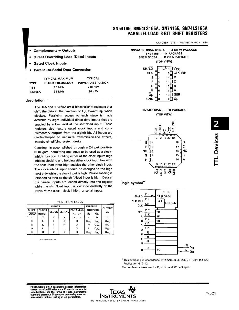
s5165a580741E6 OCTOBER 1976-REVISED MARCH 1988 Complementary Outputs JOR W PACKAGE Direct Overriding Load(Data)Inputs Gated Clock Inputs (TOP VIEW) Parallel-to-Serial Data Conversion CL 20 description PAC clocked. Par ea Th de-clamped to minimize transmission-line effects, 3272019 eby simplifying system desigr Clockingisaccomplished througha 2-input positive outs high bits clocking and holding eithe nput 三 kinhibit input should be d to the high vel only while the Paral 话兰舌 outs are loade directh into the registe ogic symbolt of the SH/LD1 UNCTION TABLE CLK INH 2 C2/ CLK SER 121 H 3 4 5 91 H 6) 1D 1984 and EC e for D.J.N.and W package 2-521 POST OFFICE BOX 655012 DALLAS.TEXAS 75265
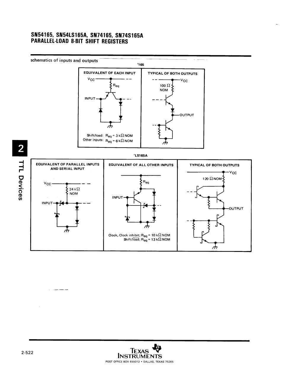
SN54165,SN54LS165A,SN74165,SN74S165A PARALLEL-LOAD 8-BIT SHIFT REGISTERS schematics of inputs and outputs EQUIVALENT OF EACH INPUT TYPICAL OF BOTH OUTPUTS -Vcc NPUT OUTPUT 2 'LS165A EQUIVALENT OF ALL OTHER INPUTS TYPICAL OF BOTH OUTPUTS TTL Devic 120 2 NOM NPU UTPU cck,ceRa:i19品N8N 2-522 A是
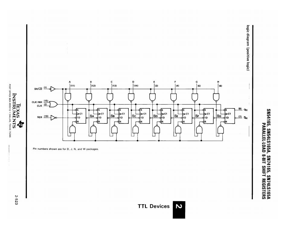
时古古古古古古 ER 110) 电围用超超: Pn numbers shown are for D.J.N.and TTL Devices
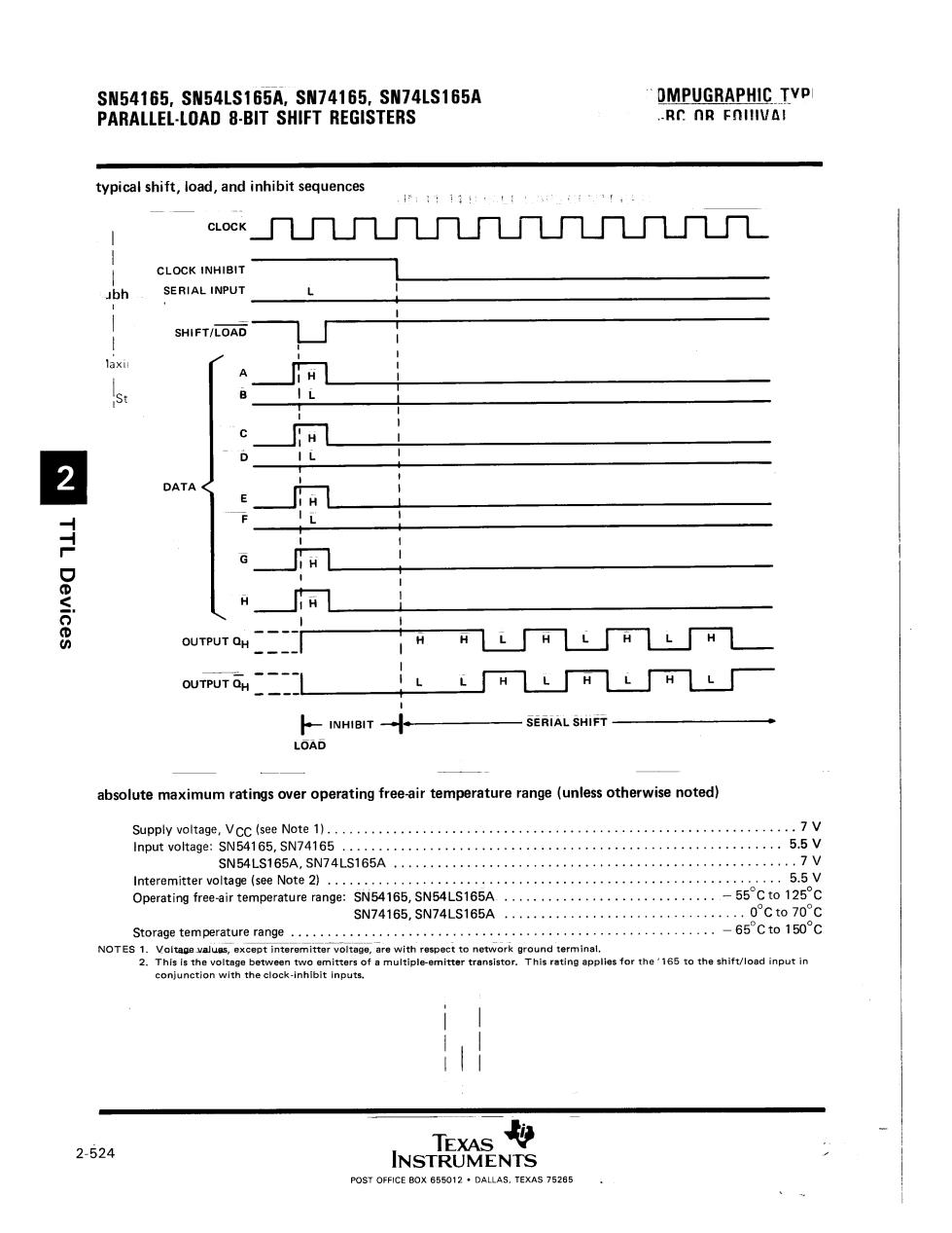
SN54165,SN54LS165A,SN74165,SN74LS165A OMPUGRAPHIC TYP PARALLEL-LOAD 8-BIT SHIFT REGISTERS .RC OR ENIlIVAI typical shift,load,and inhibit sequences 111 k冂几冂冂冂冂冂T冂冂冂冂 CLOCK INHIBIT abh SERIAL INPUT SHIFT/LOAD 2 DATA TTL Devices OUTPUT OH 0 UTPUT Qj,- INHIBIT一十 SERIAL SHIFT- LOAD absolute maximum ratings over operating free-air temperature range(unless otherwise noted) Supply voltage,Vcc (see Note 1). Input voltage:SN54165,SN74165 。,。,。gg。gg。年。g。g,。年e;,年444。get年t。4。t0。0.4 SN54LS165A,SN74LS165A. Interemitter voltage(see Note 2). ,。g。,g。g。g。年。,tt,。,。+。,。4 Operating free-air temperature range:SN54165,SN54LS165A .-55 SN74165,SN74LS165A Storage temperature range.- NOTESO valuas,except in the'165 t the hift/load input in 2-524 TEMs也 INSTRUMENTS OST OFFICE BOX 655012.DALLAS. EXAS 75265
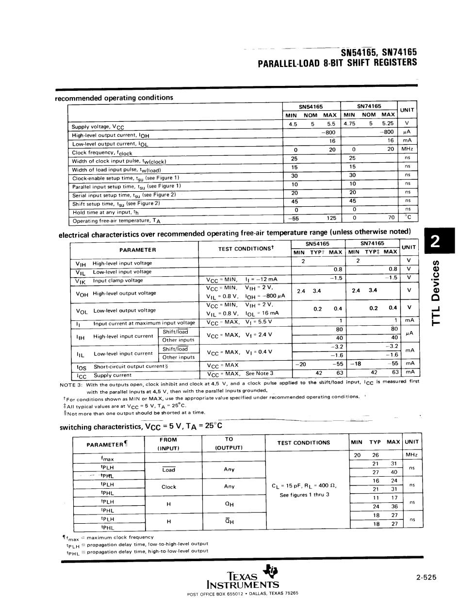
SN54165,SW74165 PARALLEL-LOAD 8-BIT SHIFT REGISTERS ommended operating conditions SN54185 SN74165 UNIT MIN NOM MAX MIN NOM MA Supply voltage.VCC 45 800 High-level o Clock frec .te 25 ns (e Figure 2) temperature.TA -55 125 lectrical characteristics over recommended operating free-air tem ure range (unless otherwise noted) N74165 PARAMETER TEST CONDITIONST MIN TYPE MAX 2 MIN TYPE MAX UNIT 2 evel input voltage 1.5 1.5 VOH High-level output voltage 2.434 24 VoL Low-level output voltage 0.20.4 0.20.4 input current at maximun mA High-level input cue 80 VCCMAX.VI-2.4V 10 32 32 L Low-level input current VCC=MAX.VI-0.4V mA lOS Short-c utput current VCC -MAX 20 —CJn。3 63 42 631 mA ply curren 268 recommended operating conditions. switching characteristics,VCC-5 V,TA-25C PARAMETER FROM TO TEST CONDITIONS MIN TYP MAX UNIT (INPUTI 2026 MHz Load Any 16 Clock Any CL=15 pF,RL-400 n See figures 1 thru 3 PLH 可H 18 27s maxim HL-P 2-525 728
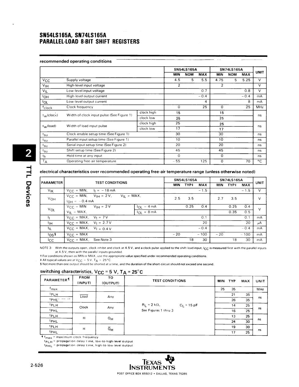
SN54LS165A.SN74LS165A PARALLEL-LOAD 8-BIT SHIFT REGISTERS recommended operating conditions SN54L5165A N74LS165A UNIT NOM NOM M out voltage 2 output current mA clock Clock frequency MHz clock high tw[clock) Width of clock input pulse (SeeFigure 1) clock lov ns Width of load put pulse ns gure 1) onut setu ure 21 2 05 ns 56 125 70 electrical characteristics over recommended operating free-air temperature range (unless otherwise noted TEST CONDITIONS 55765A 5N74565A Devices VCC MIN,18 mA -1.5 -1.5 VoH -0.4m VIH 2V. VIL MAX 2.5 3.5 27 3.5 cc MIN VIH =2V 0.250.4 0.4 VOL .25 0.35 MAXV,=7 01 mA VCC= .V=2.7 V=0.4V VCC MAX,See Note 3 18 30 18 the paralle rating conditions. nd the dueation ot the hort-ereutshouldnotexceedone switching characteristics,VCc=5 V,TA=25C PARAMETER (OUTPUT) TEST CONDITIONS MIN TYP MAX UNIT 2535 MHz ns 2 1 thru3 CL-15pF ns H QH n. tPHL ry time 2-526 NsT2N是
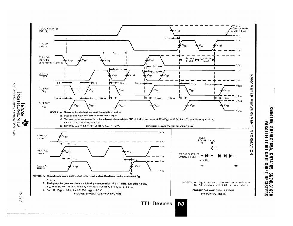
50%Zt=50n:fe165.≤10,≤10ns ≤6n IGURE 1-VOLTAGE WAVEFORMS RAMETER MEASUREMENT INFORMATION SN54165,SN54LS165A PARALLEL-LOAD OTES:A NOrEsrINn FIGURE 2-VOLTAGE WAVEFORMS pIGUngiaaesBsTfon TTL Devices

IMPORTANT NOTICE Texas Instruments(TI)reserves the right to make changes to its products or to discontinue any semiconductor product or service without notice,and advises its customers to obtain the latest version of relevant information to verify,before placing orders,that the information being relied on is current. TI warrants performance of its semico ductor products and related software to the specifications applicable a sale in accordance with TI's standard wa ranty.Testing and utilized to the extent I deems necessary to support this warranty.Specne testin of all meters oeac device is not necessarily performed,except those mandated by government requirements. Cerain app TI SEMICONDUCTOR PRODUCTS ARE NOT DESIGNED,INTENDED,AUTHORIZED,OR WARRANTED TO BE SUITABLE FOR USE IN LIFE-SUPPORT APPLICATIONS,DEVICES OR SYSTEMS OR OTHER CRITICAL APPLICATIONS. Inclusion of TI products in such applications is understood to be fully at the risk of the customer.Use of TI products in such applications requires the written approval of an appropriate TI officer.Questions concerning potential risk applications should be directed to TI through a local SC sales office. In order to minimize risks associated with the custor er's applications.adequate design and operating safeguards should be provided by the customer to minimize inherent or procedural hazards. applications atents s de ribed he n.software perfo esent that a r inte Copyright@1996.Texas Instruments Incorporated
IMPORTANT NOTICE Texas Instruments (TI) reserves the right to make changes to its products or to discontinue any semiconductor product or service without notice, and advises its customers to obtain the latest version of relevant information to verify, before placing orders, that the information being relied on is current. TI warrants performance of its semiconductor products and related software to the specifications applicable at the time of sale in accordance with TI’s standard warranty. Testing and other quality control techniques are utilized to the extent TI deems necessary to support this warranty. Specific testing of all parameters of each device is not necessarily performed, except those mandated by government requirements. Certain applications using semiconductor products may involve potential risks of death, personal injury, or severe property or environmental damage (“Critical Applications”). TI SEMICONDUCTOR PRODUCTS ARE NOT DESIGNED, INTENDED, AUTHORIZED, OR WARRANTED TO BE SUITABLE FOR USE IN LIFE-SUPPORT APPLICATIONS, DEVICES OR SYSTEMS OR OTHER CRITICAL APPLICATIONS. Inclusion of TI products in such applications is understood to be fully at the risk of the customer. Use of TI products in such applications requires the written approval of an appropriate TI officer. Questions concerning potential risk applications should be directed to TI through a local SC sales office. In order to minimize risks associated with the customer’s applications, adequate design and operating safeguards should be provided by the customer to minimize inherent or procedural hazards. TI assumes no liability for applications assistance, customer product design, software performance, or infringement of patents or services described herein. Nor does TI warrant or represent that any license, either express or implied, is granted under any patent right, copyright, mask work right, or other intellectual property right of TI covering or relating to any combination, machine, or process in which such semiconductor products or services might be or are used. Copyright 1996, Texas Instruments Incorporated