第一讲 CMOS工艺 游飞博导,副教授 电子科学与工程学院,feiyou@uestc.edu.cn
第一讲 CMOS工艺 游飞 博导,副教授 电子科学与工程学院, feiyou@uestc.edu.cn
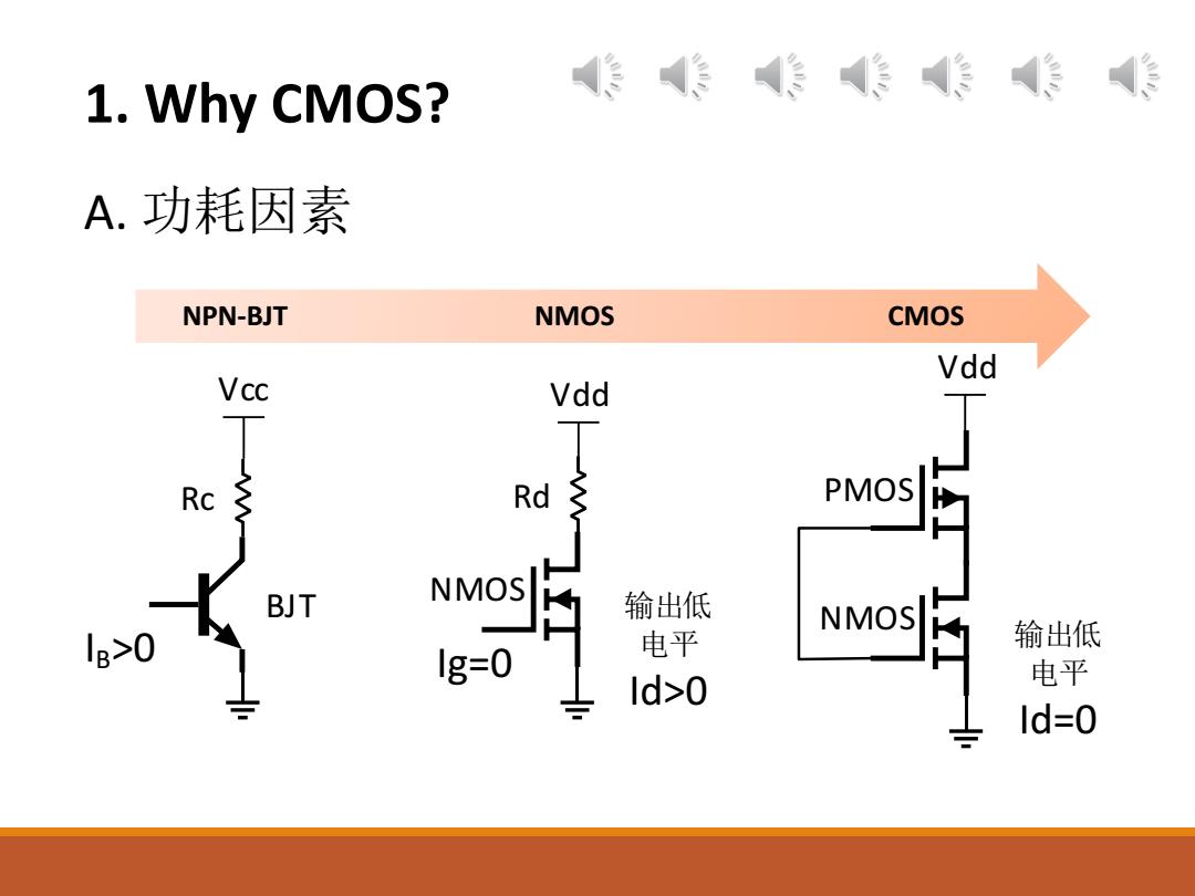
1.Why CMOS? 作传作传作 A.功耗因素 NPN-BJT NMOS CMOS Vdd Vcc Vdd Rc Rd PMOS BJT NMOS 输出低 NMOS 8>0 Ig=0 电平 输出低 Id>0 电平 Id=0
1. Why CMOS? BJT NMOS Rc Vcc Rd Vdd I B >0 Ig=0 输出低 电平 Id>0 NMOS Vdd 输出低 电平 Id=0 PMOS A. 功耗因素 NPN-BJT NMOS CMOS
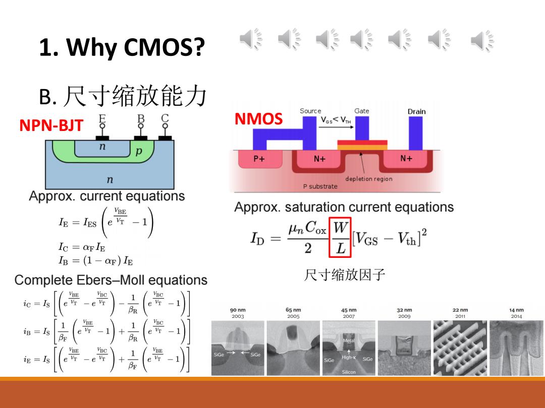
1.Why CMOS? 作作作作作 B.尺寸缩放能力 Source Gate Drain NPN-BJT NMOS VGs<VTH P+ N+ N+ n depletion region P substrate Approx.current equations VBE Approx.saturation current equations Ie=Ies ID= Hn Cox Ic OF IE 2 H[Vas -Vi]2 IB =(1-aF)IE Complete Ebers-Moll equations 尺寸缩放因子 VBE C ic Is -e VT 1 R 90 nm 65 nm 45 nm 32 nm 22nm 14nm 2003 2005 2007 2009 2011 2014 1 VBE 1 VBC iB=Is e vr -1 十 e vr 厥 分 1 -e vr SiGe VT SiGe
1. Why CMOS? B. 尺寸缩放能力 NPN-BJT Complete Ebers–Moll equations Approx. current equations NMOS Approx. saturation current equations 尺寸缩放因子

1.Why CMOS? C.集成度 Johnson figure of merit 。截止频率*击穿电压 104 High-Performance Ill-V GaN OSHEMT DARPA COSMOS InP HBT (OAZH5) 103 InP GaAs MESFET HEMT ASiGe 102 HBT 日0a Si MOSFET 10 1001011021031041051061071081091010 Number of Transistors
1. Why CMOS? C. 集成度 • Johnson figure of merit • 截止频率*击穿电压
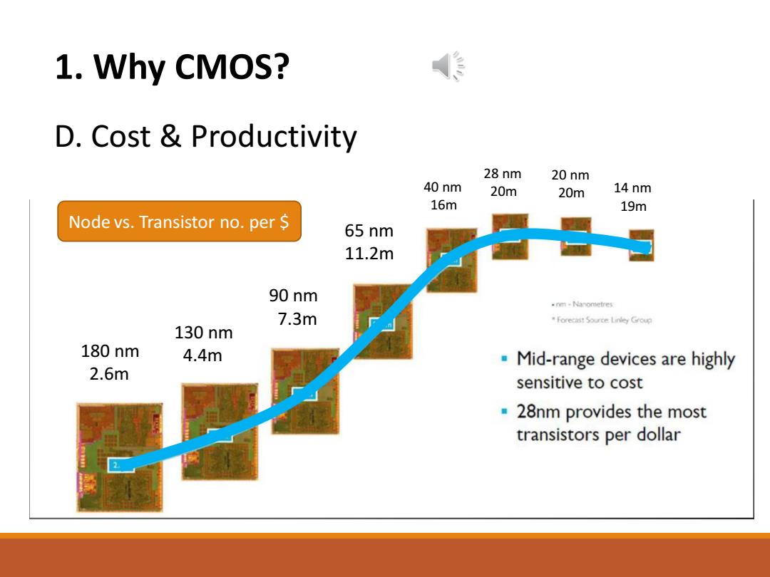
1.Why CMOS? 传 D.Cost Productivity 28 nm 20nm 40nm 20m 20m 14 nm 16m 19m Node vs.Transistor no.per S 65 nm 11.2m 90 nm .nm -Nanometres 7.3m .Forecast Source Linley Group 130nm 180nm 4.4m Mid-range devices are highly 2.6m sensitive to cost 28nm provides the most transistors per dollar
1. Why CMOS? D. Cost & Productivity 180 nm 2.6m 130 nm 4.4m 90 nm 7.3m 65 nm 11.2m 40 nm 16m 28 nm 20m 20 nm 20m 14 nm 19m Node vs. Transistor no. per $
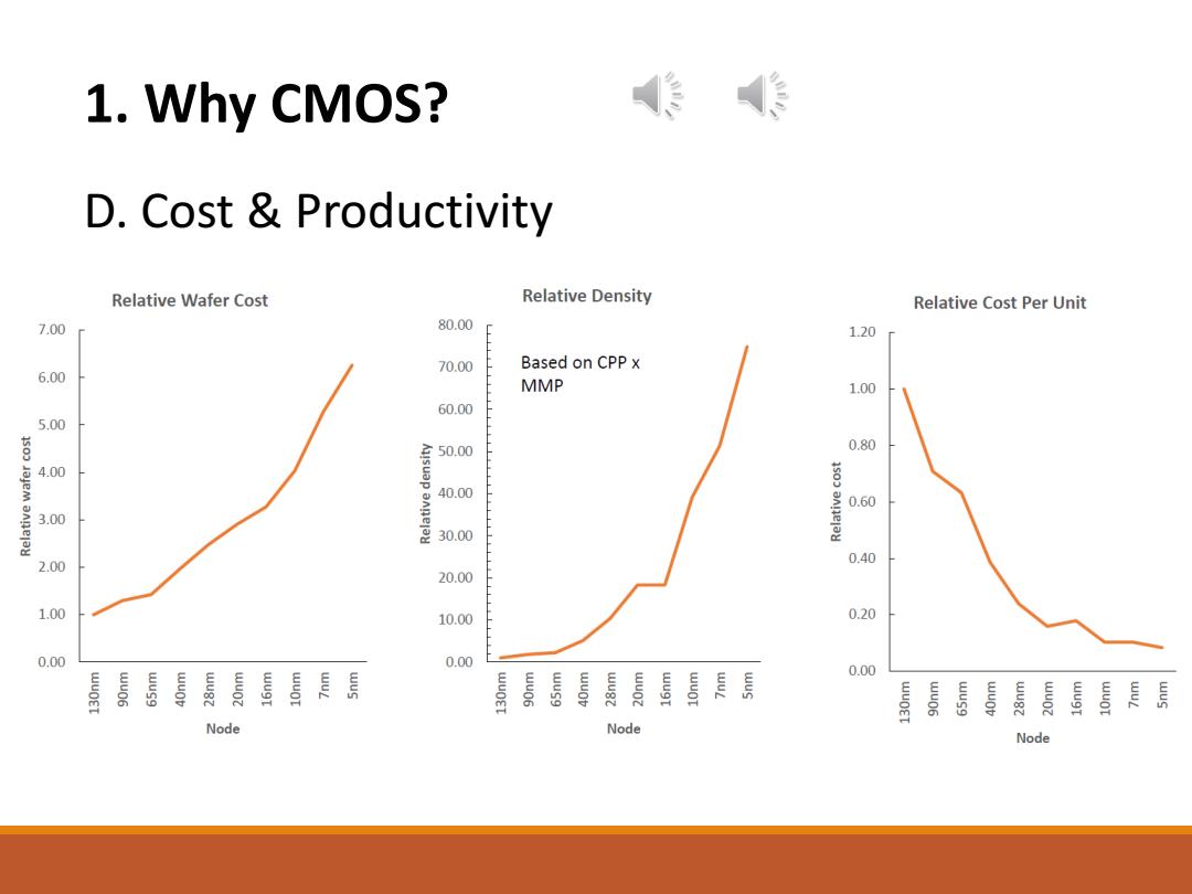
1.Why CMOS? 作 D.Cost Productivity Relative Wafer Cost Relative Density Relative Cost Per Unit 7.00 80.00 1.20 70.00 Based on CPP x 6.00 MMP 1.00 60.00 5.00 0.80 4.00 40.00 0.60 3.00 30.00 2.00 0.40 20.00 1.00 10.00 020 0.00 0.00 0.00 Node Node Node
1. Why CMOS? D. Cost & Productivity
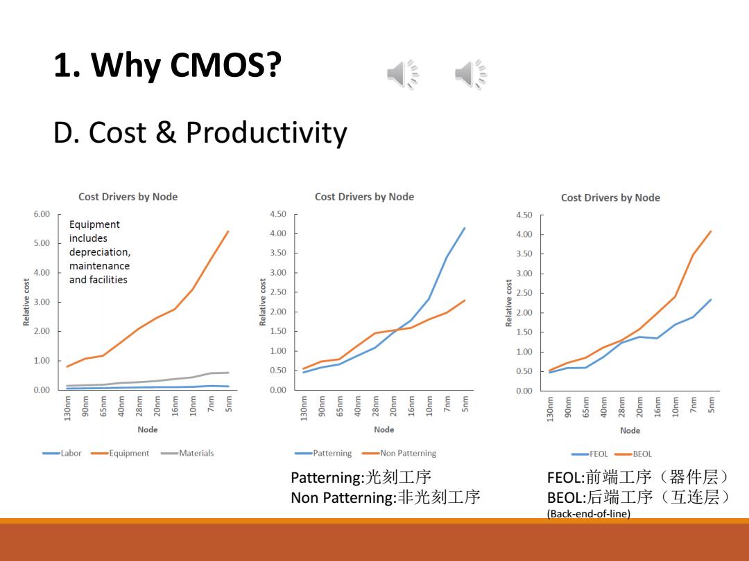
1.Why CMOS? D.Cost Productivity Cost Drivers by Node Cost Drivers by Node Cost Drivers by Node 6.00 4.50 4.50 Equipment includes 4.00 4.00 5.00 depreciation, 3.50 3.50 maintenance 4.00 3.00 3.00 and facilities 2.50 3.00 2.00 annelay 2.00 2.00 1.50 1.50 1.00 1.00 1.00 0.50 0.50 0.00 0.00 0.00 Node Node Node Equipment Materials -Patterning -Non Patterning Patterning:光刻工序 FEOL:前端工序(器件层) Non Patterning:非光刻工序 BEOL:后端工序(互连层) (Back-end-of-line)
1. Why CMOS? D. Cost & Productivity Patterning:光刻工序 Non Patterning:非光刻工序 FEOL:前端工序(器件层) BEOL:后端工序(互连层) (Back-end-of-line)

2.CMOS Process 传 Poly G B S D Oxide p W p+ n+ nt Leff p-substrate -drawn
2. CMOS Process
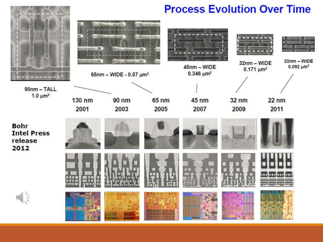
Process Evolution Over Time 32nm-WIDE 22nm-WIDE 45nm-WIDE 0.171m2 0.0924m2 65nm-WIDE-0.57 um2 0.346μm2 90nm-TALL 1.0μm2 130nm 90 nm 65 nm 45 nm 32 nm 22 nm 2001 2003 2005 2007 2009 2011 Bohr Intel Press release 2012
2. CMOS Process
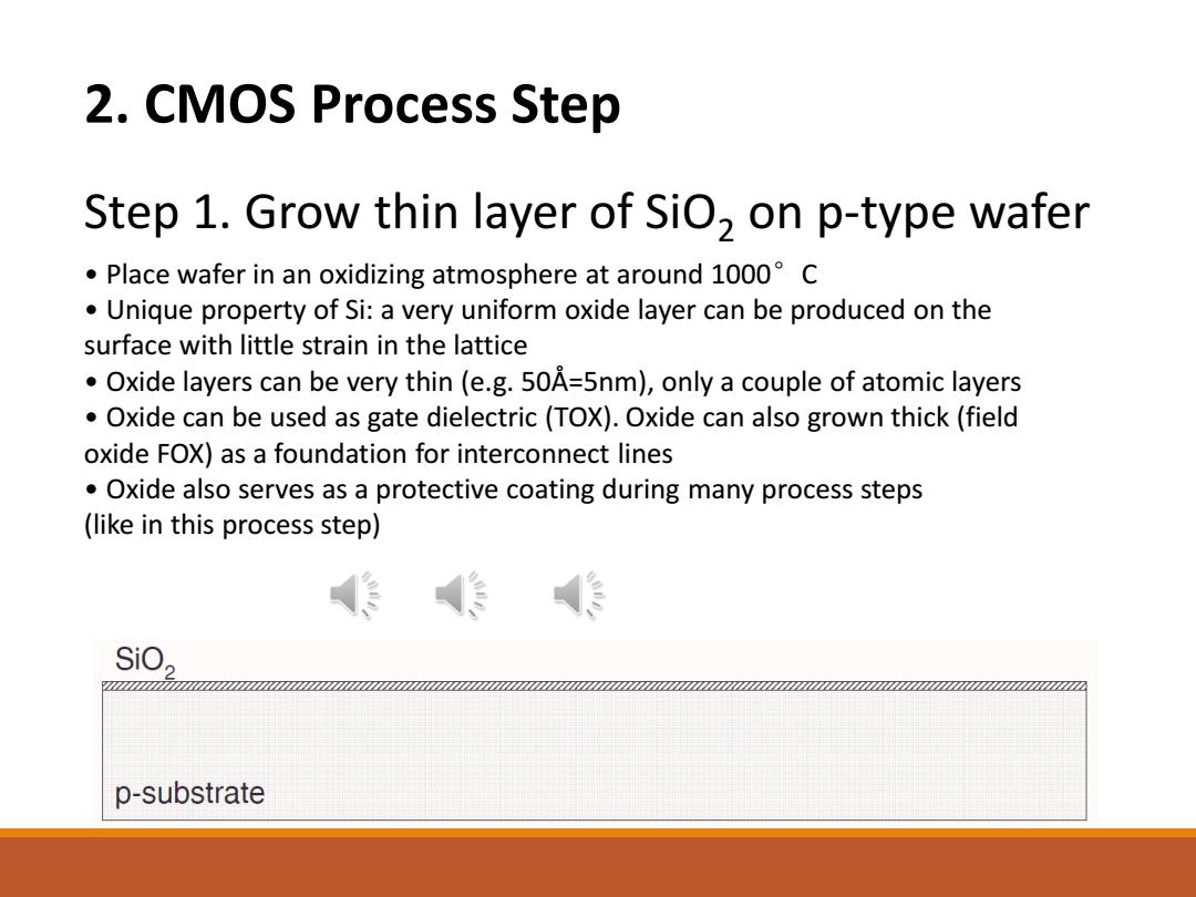
2.CMOS Process Step Step 1.Grow thin layer of SiO,on p-type wafer Place wafer in an oxidizing atmosphere at around 1000C Unique property of Si:a very uniform oxide layer can be produced on the surface with little strain in the lattice Oxide layers can be very thin (e.g.50A=5nm),only a couple of atomic layers Oxide can be used as gate dielectric(TOX).Oxide can also grown thick(field oxide FOX)as a foundation for interconnect lines Oxide also serves as a protective coating during many process steps (like in this process step) SiO, p-substrate
2. CMOS Process Step Step 1. Grow thin layer of SiO2 on p-type wafer • Place wafer in an oxidizing atmosphere at around 1000°C • Unique property of Si: a very uniform oxide layer can be produced on the surface with little strain in the lattice • Oxide layers can be very thin (e.g. 50Å=5nm), only a couple of atomic layers • Oxide can be used as gate dielectric (TOX). Oxide can also grown thick (field oxide FOX) as a foundation for interconnect lines • Oxide also serves as a protective coating during many process steps (like in this process step)