
第九讲 Power Amplifiers 游飞博导/副教授,电子科技大学 feiyou@uestc.edu.cn 1
第九讲 Power Amplifiers 游飞 博导/副教授,电子科技大学 feiyou@uestc.edu.cn
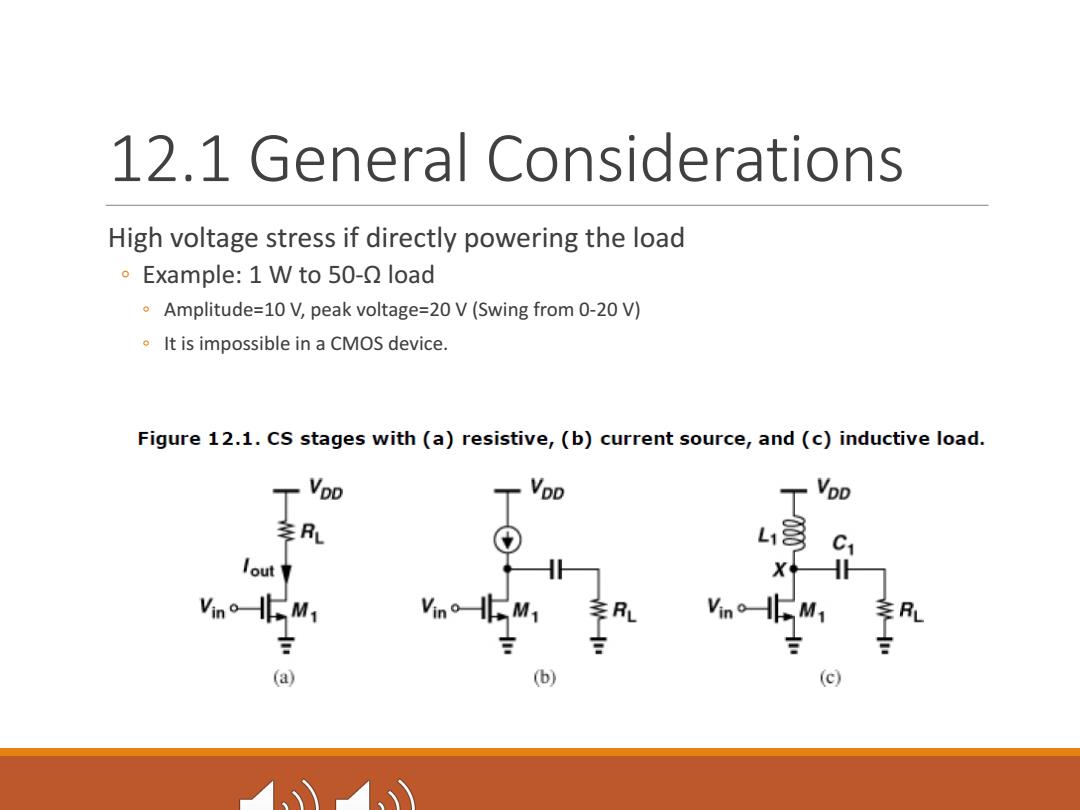
12.1 General Considerations High voltage stress if directly powering the load Example:1 W to 50-Q load Amplitude=10 V,peak voltage=20 V(Swing from 0-20 V) It is impossible in a CMOS device. Figure 12.1.CS stages with (a)resistive,(b)current source,and (c)inductive load. T 多RL L1 C1 x H M Vin vn。H M1 幸R (a) (c
12.1 General Considerations High voltage stress if directly powering the load ◦ Example: 1 W to 50-Ω load ◦ Amplitude=10 V, peak voltage=20 V (Swing from 0-20 V) ◦ It is impossible in a CMOS device
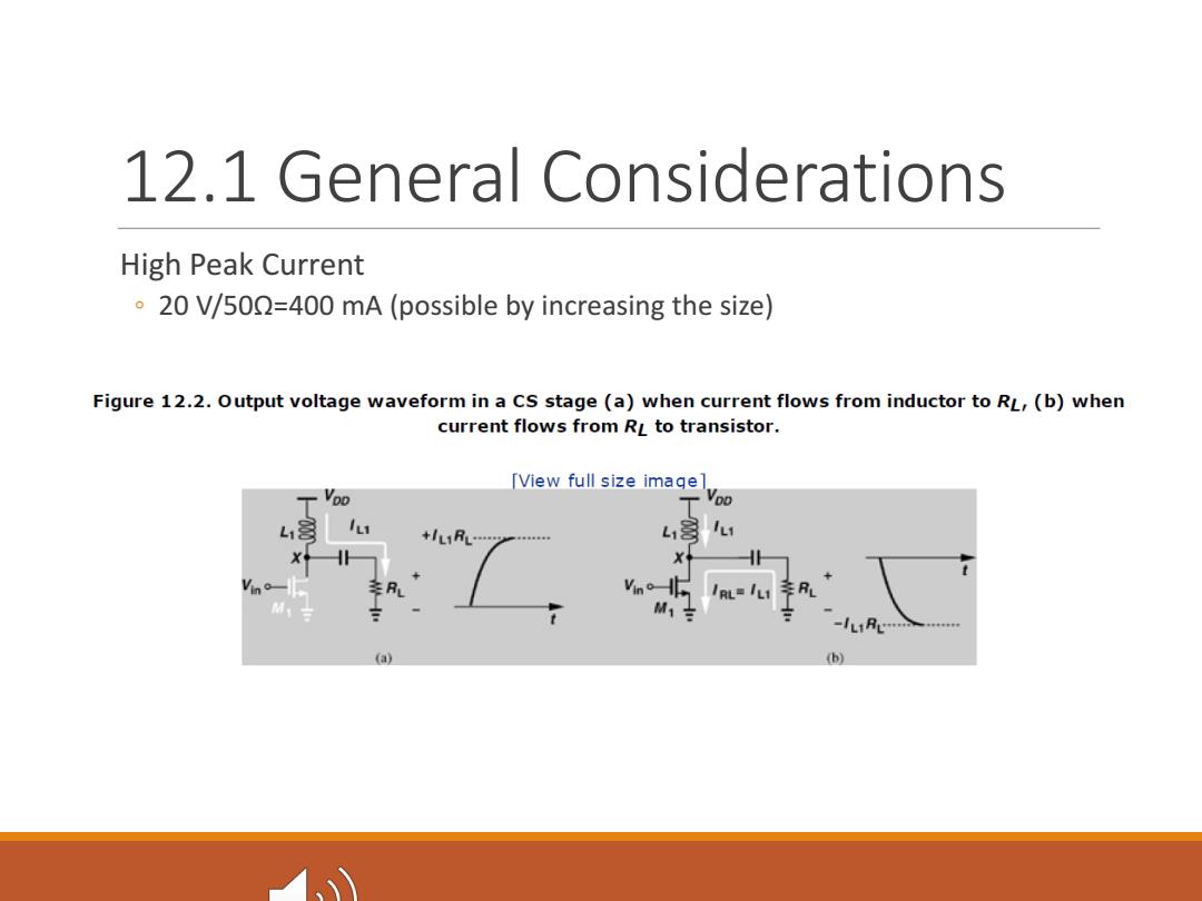
12.1 General Considerations High Peak Current 20 V/500=400 mA(possible by increasing the size) Figure 12.2.Output voltage waveform in a Cs stage (a)when current flows from inductor to RL,(b)when current flows from RL to transistor. [View full size image] VoD X M M1 (3 (b)
12.1 General Considerations High Peak Current ◦ 20 V/50Ω=400 mA (possible by increasing the size)
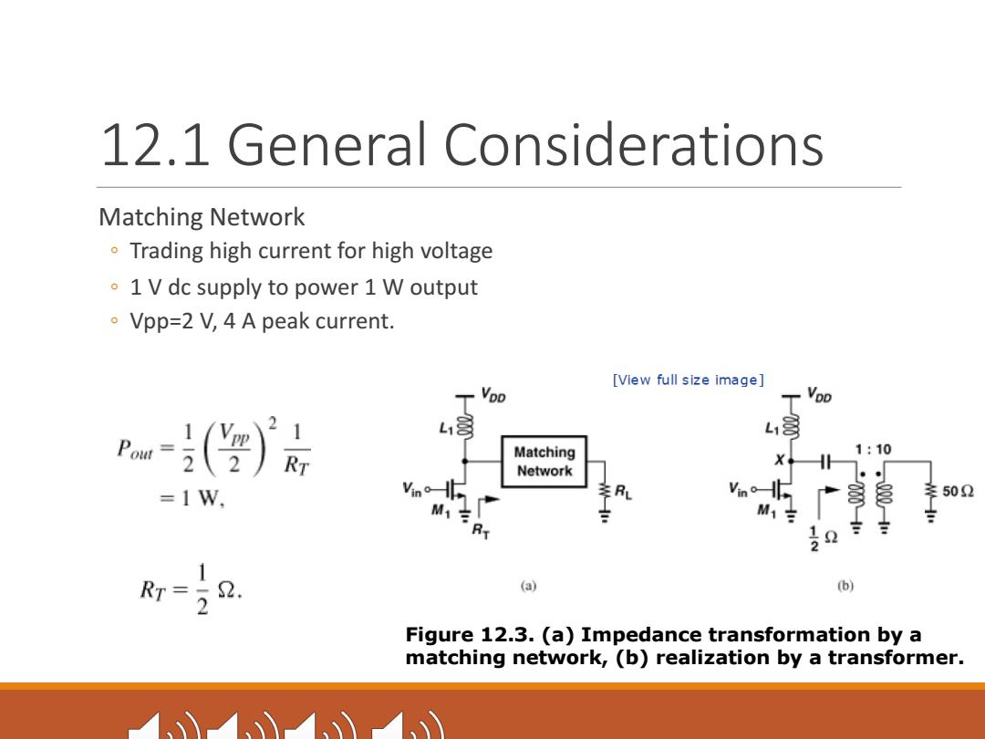
12.1 General Considerations Matching Network Trading high current for high voltage .1 V dc supply to power 1 W output Vpp=2 V,4 A peak current. [View full size image] Matching 1:10 Network =1W. 50 M11 RT= -2 (a) b Figure 12.3.(a)Impedance transformation by a matching network,(b)realization by a transformer
12.1 General Considerations Matching Network ◦ Trading high current for high voltage ◦ 1 V dc supply to power 1 W output ◦ Vpp=2 V, 4 A peak current. Figure 12.3. (a) Impedance transformation by a matching network, (b) realization by a transformer
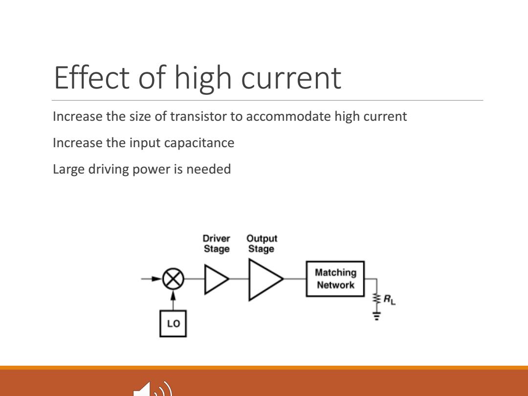
Effect of high current Increase the size of transistor to accommodate high current Increase the input capacitance Large driving power is needed Driver Output Stage Stage Matching Network 季RL LO
Effect of high current Increase the size of transistor to accommodate high current Increase the input capacitance Large driving power is needed
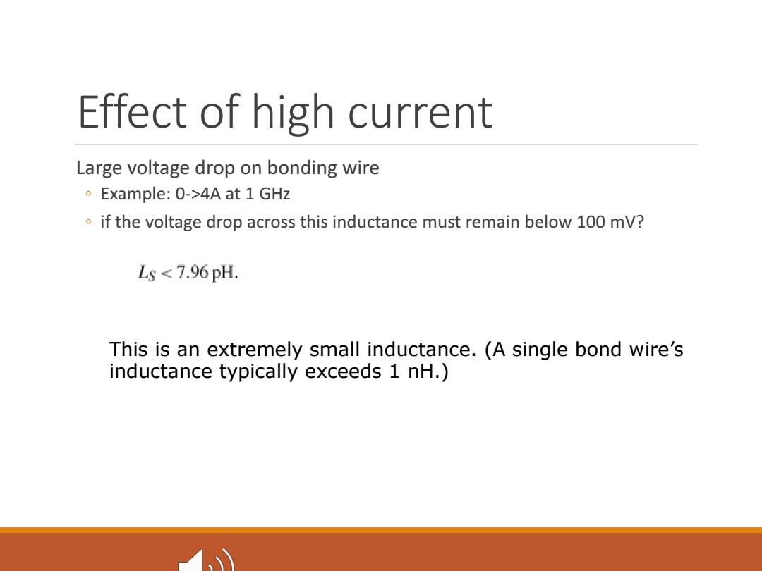
Effect of high current Large voltage drop on bonding wire Example:0->4A at 1 GHz if the voltage drop across this inductance must remain below 100 mV? Ls<7.96pH. This is an extremely small inductance.(A single bond wire's inductance typically exceeds 1 nH
Effect of high current Large voltage drop on bonding wire ◦ Example: 0->4A at 1 GHz ◦ if the voltage drop across this inductance must remain below 100 mV? This is an extremely small inductance. (A single bond wire’s inductance typically exceeds 1 nH.)
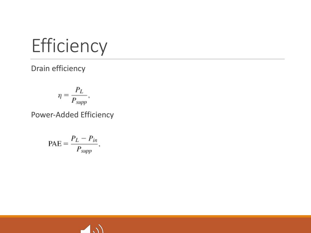
Efficiency Drain efficiency PL 升= Psupp Power-Added Efficiency PAE=PL -P'm Psupp
Efficiency Drain efficiency Power-Added Efficiency
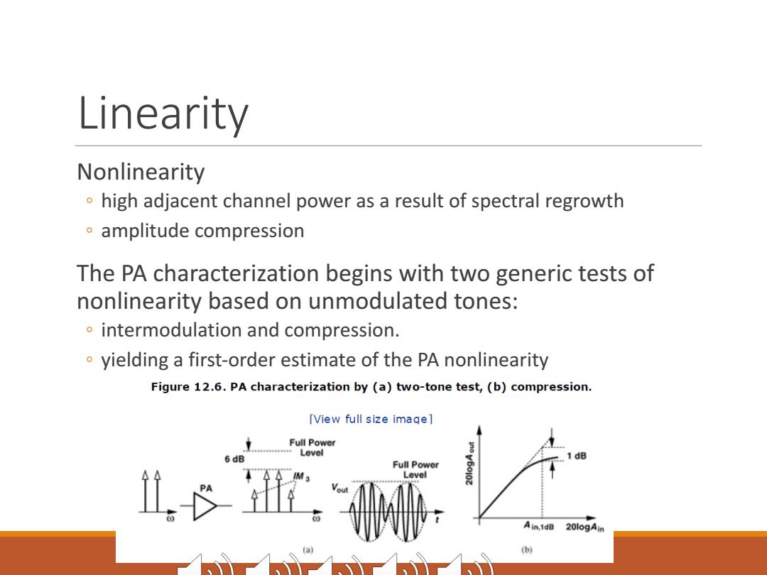
Linearity Nonlinearity high adjacent channel power as a result of spectral regrowth amplitude compression The PA characterization begins with two generic tests of nonlinearity based on unmodulated tones: intermodulation and compression. yielding a first-order estimate of the PA nonlinearity Figure 12.6.PA characterization by (a)two-tone test,(b)compression. [View full size imagel Full Power Level Full Power Level Ain,1dB 20logAin (b)
Linearity Nonlinearity ◦ high adjacent channel power as a result of spectral regrowth ◦ amplitude compression The PA characterization begins with two generic tests of nonlinearity based on unmodulated tones: ◦ intermodulation and compression. ◦ yielding a first-order estimate of the PA nonlinearity
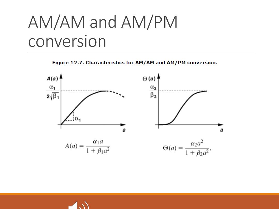
AM/AM and AM/PM conversion Figure 12.7.Characteristics for AM/AM and AM/PM conversion. A(a) 日(a) 2师 影 01 a a aja A(a)= 2a2 1+B1a2 ⊙(@)= 1+2a21
AM/AM and AM/PM conversion

Single-Ended and Differential PAS Most stand-alone PAs have been designed as a cascade of single-ended stages.Two reasons account for this choice: the antenna is typically single-ended, and single-ended RF circuits are much simpler to test than their differential counterparts. Drawbacks First,they "waste"half of the transmitter voltage gain Large current induced feedback
Single-Ended and Differential PAs Most stand-alone PAs have been designed as a cascade of single-ended stages. Two reasons account for this choice: ◦ the antenna is typically single-ended, ◦ and single-ended RF circuits are much simpler to test than their differential counterparts. Drawbacks ◦ First, they “waste” half of the transmitter voltage gain ◦ Large current induced feedback