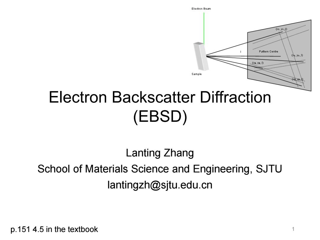
Electron Beam 11D Pattern Centre 4.y4,D 的,归D Sample Electron Backscatter Diffraction (EBSD) Lanting Zhang School of Materials Science and Engineering,SJTU lantingzh@sjtu.edu.cn p.151 4.5 in the textbook
Electron Backscatter Diffraction (EBSD) Lanting Zhang School of Materials Science and Engineering, SJTU lantingzh@sjtu.edu.cn p.151 4.5 in the textbook 1

Microstructure of a high-N2,high-Mn(P506- type)austenitic stainless steel 2
Microstructure of a high-N2 , high-Mn (P506- type) austenitic stainless steel 2
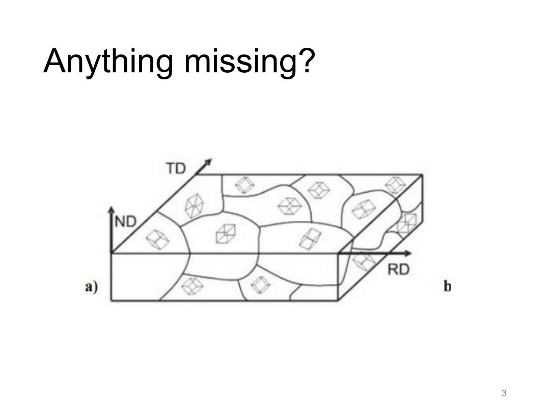
Anything missing? TD IND ① 8 RD a ⑧ b 3
Anything missing? 3
Anything missing? Chemical information Crystallographic information ·Else?
Anything missing? • Chemical information • Crystallographic information • Else? 4
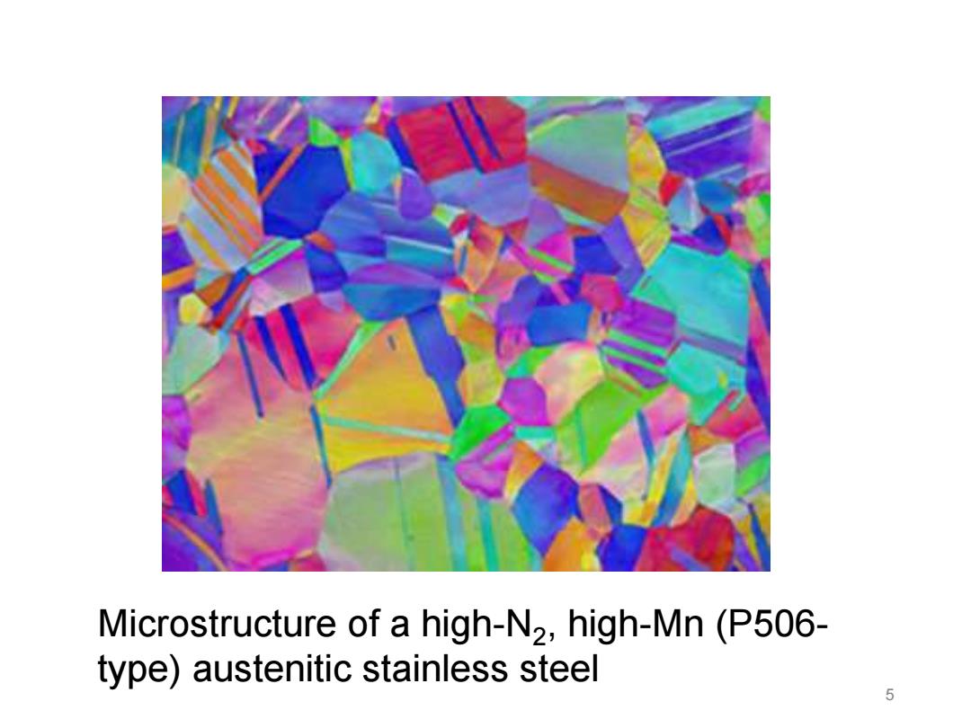
Microstructure of a high-N2,high-Mn(P506- type)austenitic stainless steel 5
Microstructure of a high-N2 , high-Mn (P506- type) austenitic stainless steel 5
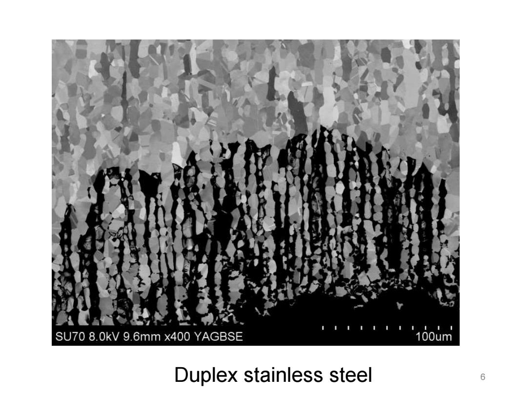
SU70 8.0kV 9.6mm x400 YAGBSE 100um Duplex stainless steel 6
Duplex stainless steel 6
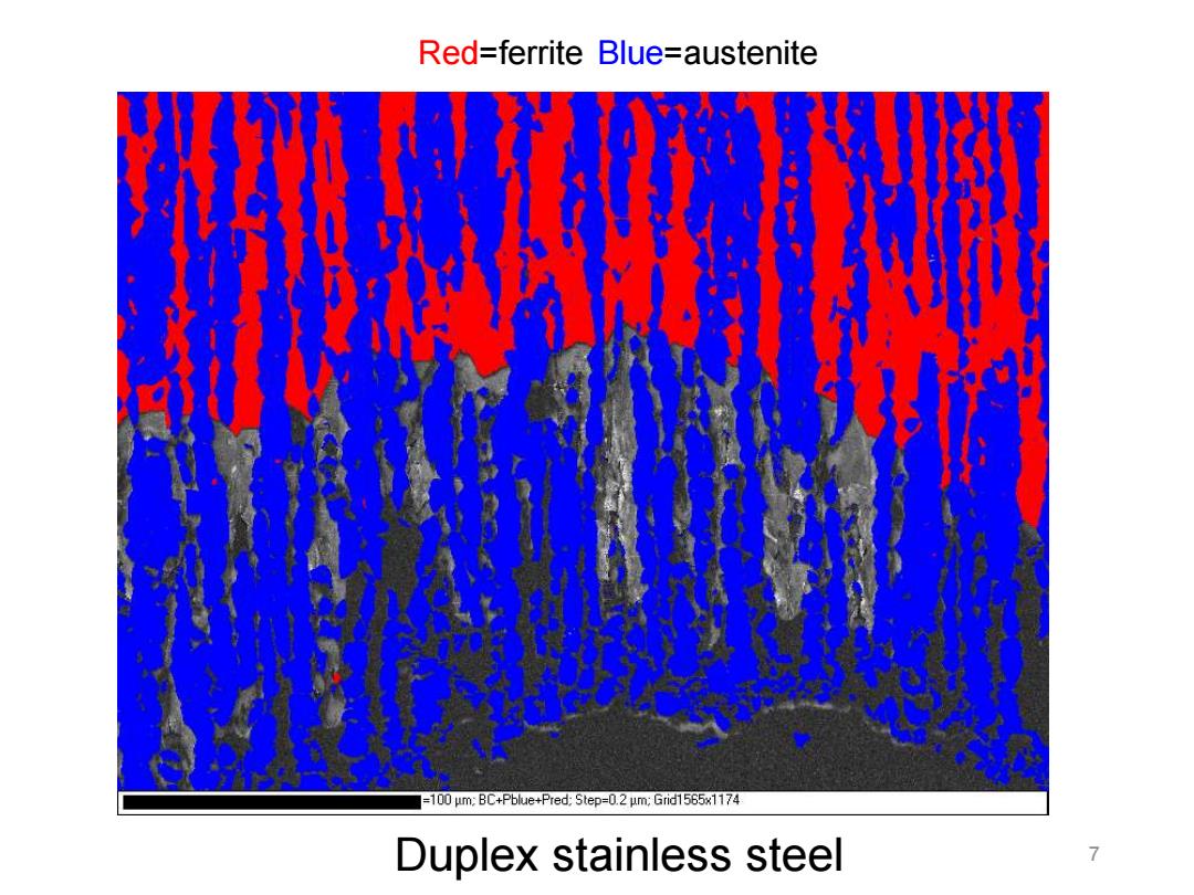
Red=ferrite Blue=austenite =100 um:BC+Pblue+Pred:Step=0.2 um;Grid1565x1174 Duplex stainless steel 7
Duplex stainless steel 7 Red=ferrite Blue=austenite
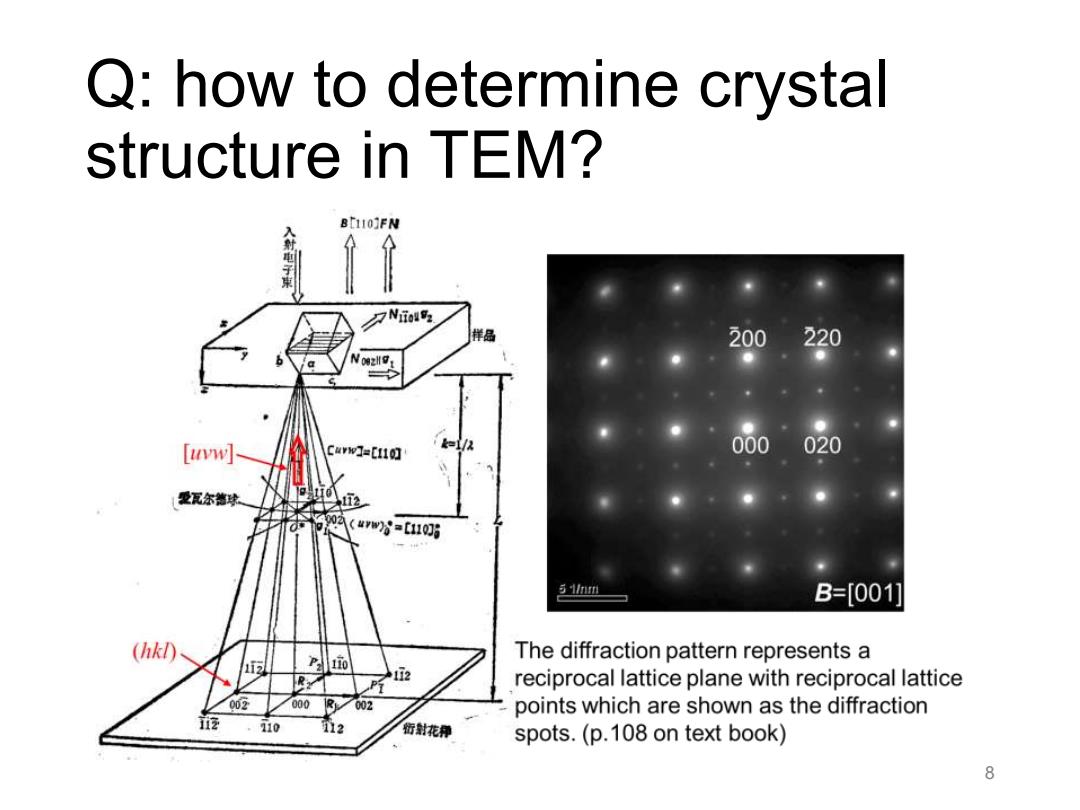
Q:how to determine crystal structure in TEM? BT110JFN 入耕电子束 Niiol92 样品 20 220 [- Cayw=[I1】 000 020 爱瓦尔德球 5 1/nm B=[001] (hkl The diffraction pattern represents a 1i2 1i2 reciprocal lattice plane with reciprocal lattice 002 000 R 002 points which are shown as the diffraction 110 112 衍射花种 spots.(p.108 on text book) 8
Q: how to determine crystal structure in TEM? 8
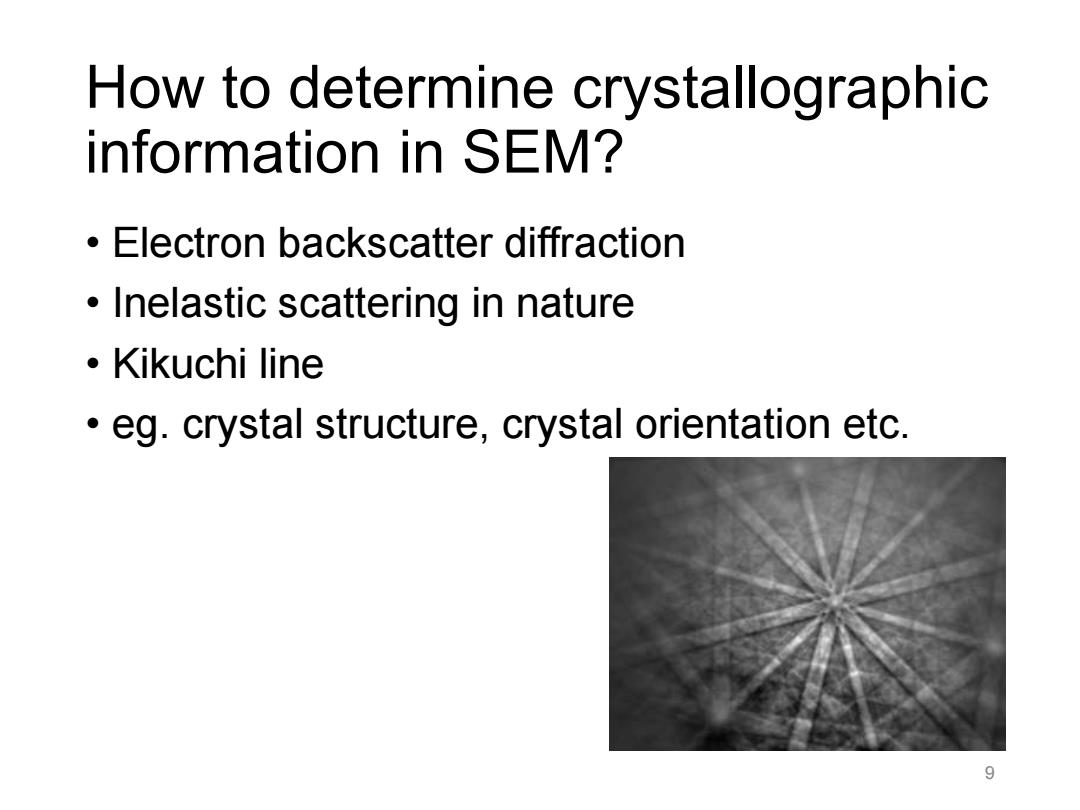
How to determine crystallographic information in SEM? Electron backscatter diffraction Inelastic scattering in nature ·Kikuchi line eg.crystal structure,crystal orientation etc. 9
How to determine crystallographic information in SEM? • Electron backscatter diffraction • Inelastic scattering in nature • Kikuchi line • eg. crystal structure, crystal orientation etc. 9

Kikuchi Patterns in TEM&EBSD incident incident TEM incident electron beam EBSD phosphor electron beam Kossel- electron beam screen cones diffuse scattering sample sample Kossel- lattice cones planes(hkl) tilted 90°.0 lattice sample planes(hkl) ]26 Kikuchi-lines lattice planes (hkl) Kikuchi-lines excess-defect- Kikuchi-line (Courtesy of Dr Ke Chen) 10
Kikuchi Patterns in TEM & EBSD (Courtesy of Dr Ke Chen) 10