To conclude 1 ●●● ●●●● ●●●●● 5.1 Filter Design by the Insertion Loss Method ●●●0 ●●●●0 PLR ● Power Loss ratio: ● Equal ● ripple Pn= 1 PLR= PLood 1-T() Maximally fat Maximally flat response(Butterworth) 05 1.0 1.5 ww. (for0>>0) 8N+1=1 R0=80=1 =8别 W-0 YY Equal-ripple response (Chebyshev) 宁C=81 卡C3=8的 Px=1+kT (for @>0.) Nis odd, 8w+1=1 \2N Limear phase response:( is even,gw+l≠l The group delay) 1
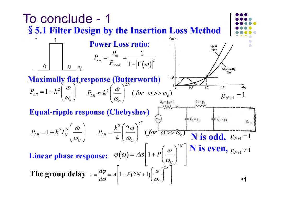
To conclude - 1 §5.1 Filter Design by the Insertion Loss Method Power Loss ratio: Maximally flat response (Butterworth) Equal-ripple response (Chebyshev) Linear phase response: The group delay N is odd, N is even, •1 2 1 1 in LR Load P P P 2 2 1 N LR c P k 2 2 ( ) N LR c c P k for 1 1 N g 2 2 1 LR N C P kT 2 2 2 ( ) 4 N LR c C k P for 1 1 N g 1 1 N g 2 1 N C A P 2 1 21 N C d A PN d
PLR To conciude 2 Equal ripple 5.2 Filter Scaling and Transformation PL典 flat 1+k C Ck R0=80=1 =8 RoWc M-o- 0 LPF G8 卡C=8 -←→0 00 ←→0 -101 HPF 00 PLR PLR BSF 00 ,=@0,生 02-0 BPF 00 @ok 00 AC C元 △*00 OLk 入*0g
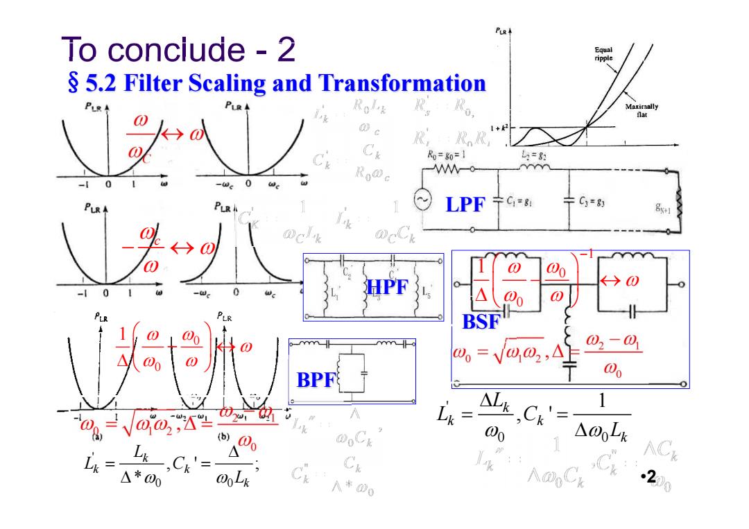
To conclude - 2 LPF BSF HPF BPF §5.2 Filter Scaling and Transformation ' 0 0 ,' ; *k k k k L L C L ' 0 0 1 , ' k k k k L L C L •2 c 0 0 1 1 0 0 1
To conclude 3 ●●● ●●●● ●●●●● ●●●● 1.Richard's Transformation L,Ctransmission line ●●●●0 ●●●● 2=gBl=g(ol/yp):2→ol1→1→gB1=1→1=元/8ato。° 2.Kuroda's Identities (for LPF and BSF) Series stub->shunt stub. 1 L=33487L=33487 500 502 Mom YYY-9 21752 21750 ÷C=0.717 64.90 70.3Q 6.90 a 3.K-J Inverter (for BPF and BSF): Series Resonator->shunt resonator. 一A/4 A/4 Zo=K Yo=J K=1/wC J=WC 3
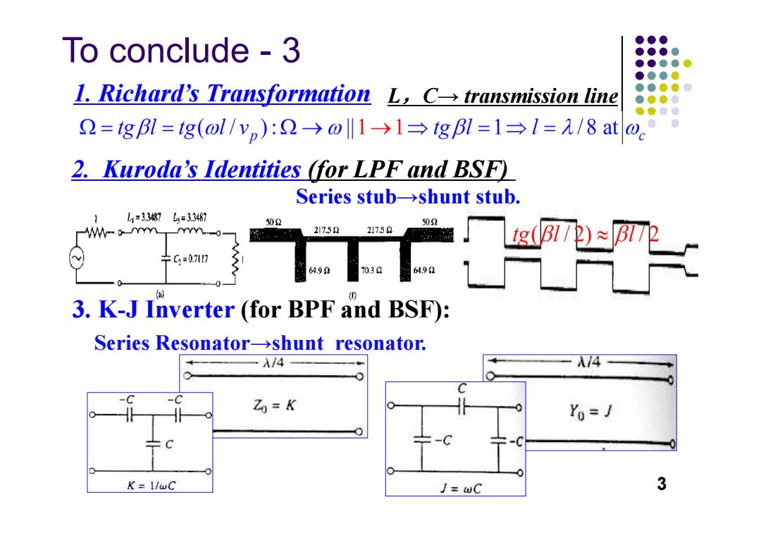
To conclude - 3 1. Richard’s Transformation 2. Kuroda’s Identities (for LPF and BSF) L,C→ transmission line Series stub→shunt stub. 3 3. K-J Inverter (for BPF and BSF): Series Resonator→shunt resonator
●●● ●●●● Microwave and RF ●●●● ●●●● ●●●●0 ●●●● ●●●● Design of Wireless ● Systems Chapter 6 Amplifiers 放大器 Dr.Xian Qi Lin 5
Microwave and RF Design of Wireless Systems Chapter 6 Dr. Xian Qi Lin Amplifiers 放大器 5
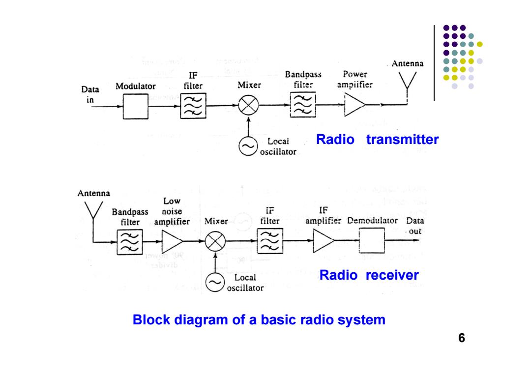
●●● ●●●● ●●●●心 ●●●● Antenna ●●●●0 ●●●● IF Bandpass Power ●●●● Data Modulator filter Mixer filter ampiifier ● in Local Radio transmitter oscillator Antenna Low Bandpass noise F IF filter amplifier Mixer filter amplifier Demedulator Data out Local Radio receiver oscillator Block diagram of a basic radio system 6
Radio transmitter Block diagram of a basic radio system Radio receiver 6
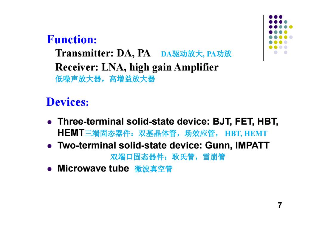
●●● ●●●● ●●●● ●●●● Function: ●●●● ●●●● ●●●● Transmitter:DA,PADA驱动放大,PA功放 ●● Receiver:LNA,high gain Amplifier 低噪声放大器,高增益放大器 Devices: Three-terminal solid-state device:BJT,FET,HBT, HEMT三端固态器件:双基晶体管,场效应管,HBT,HEMT Two-terminal solid-state device:Gunn,IMPATT 双端口固态器件:耿氏管,雪崩管 ●Microwave tube微波真空管 7
Three-terminal solid-state device: BJT, FET, HBT, HEMT三端固态器件:双基晶体管,场效应管, HBT, HEMT Two-terminal solid-state device: Gunn, IMPATT 双端口固态器件:耿氏管,雪崩管 Microwave tube 微波真空管 Transmitter: DA, PA DA驱动放大, PA功放 Receiver: LNA, high gain Amplifier 低噪声放大器,高增益放大器 Function: Devices: 7
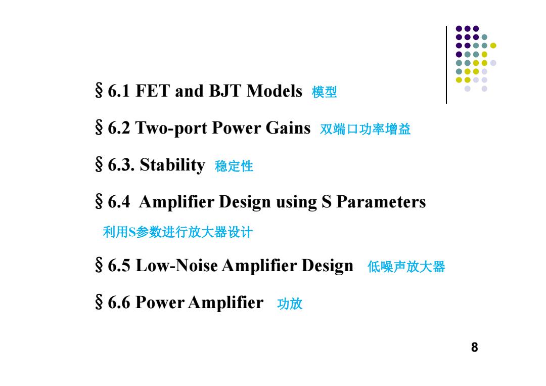
●●】 ●●●● ●●●●● ●●●0 ●●●●0 ●●●● ●●●● §6.1 FET and BJT Models模型 ●● §6.2Two-port Power Gains双端口功率增益 §6.3.Stability稳定性 6.4 Amplifier Design using S Parameters 利用$参数进行放大器设计 6.5 Low-Noise Amplifier Design 1低噪声放大器 §6.6 Power Amplifier功放 8
§6.1 FET and BJT Models 模型 §6.2 Two-port Power Gains 双端口功率增益 §6.3. Stability 稳定性 §6.4 Amplifier Design using S Parameters 利用S参数进行放大器设计 §6.5 Low-Noise Amplifier Design 低噪声放大器 §6.6 Power Amplifier 功放 8
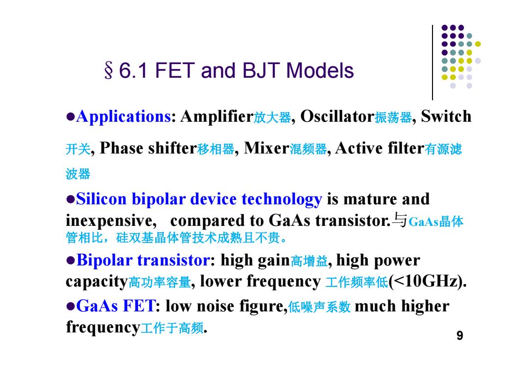
●●● ●●● ●●●● ●●●● ●●●● §6.1 FET and BJT Models ●●●0 Applications:Amplifier放大器,Oscillator振荡器,Switch 开关,Phase shifter移相器,Mixer混频器,Active filter有源滤 波器 Silicon bipolar device technology is mature and inexpensive,compared to Gaas transistor.与GaAs晶体 管相比,硅双基晶体管技术成熟且不贵。 ●Bipolar transistor:high gain高增益,high power capacity高功率容量,lower frequency工作频率低(<10GHz). ●GaAs FET:low noise figure,.低噪声系数much higher frequency工作于高频. 9
§6.1 FET and BJT Models Applications: Amplifier放大器, Oscillator振荡器, Switch 开关, Phase shifter移相器, Mixer混频器, Active filter有源滤 波器 Silicon bipolar device technology is mature and inexpensive, compared to GaAs transistor.与GaAs晶体 管相比,硅双基晶体管技术成熟且不贵。 Bipolar transistor: high gain高增益, high power capacity高功率容量, lower frequency 工作频率低(<10GHz). GaAs FET: low noise figure,低噪声系数 much higher frequency工作于高频. 9
●●● ●●●● ●●●●● ●●●0 1.FET △。1●0 D● ① Voltage device.电压器件 )0 耗尽层 ② GaAs has higher electron mobility, D N外延层 高电子迁移率(compared to silicon) ③ Low noise figure,低噪声系数 半绝缘GaAs基片 Fmim≈0.35dB ④ Higher方= 8m nC. gate length栅长0,15~0.25um ⑤ Operating teequey: C ⑥ Operating point:low noise amplifier Acommon-source configuration R:(串联栅极电阻)=7D las≈0.15lass;power amplifier lds≈0.5ldss R.(漏-源极电阻)=4002 C,(栅-源极电容)=0.3pF ⑦ DC biased直流偏置 C.(漏-源极电容)=0.12pF Ca(栅-漏极电容)-0.01pF gm(跨导)-40mS 10
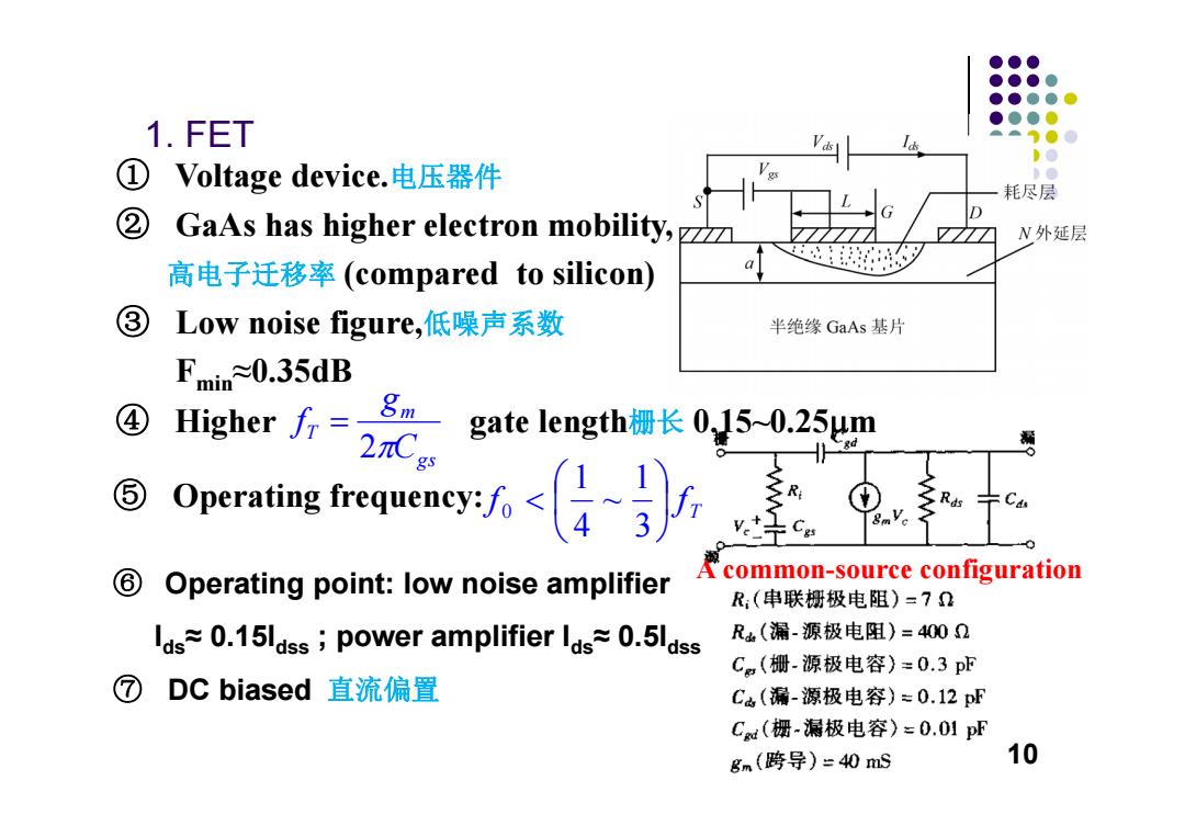
1. FET ⑥ Operating point: low noise amplifier Ids≈ 0.15Idss ; power amplifier Ids≈ 0.5Idss ⑦ DC biased 直流偏置 ① Voltage device.电压器件 ② GaAs has higher electron mobility, 高电子迁移率 (compared to silicon) ③ Low noise figure,低噪声系数 Fmin≈0.35dB gs m T C g f 2 ④ Higher gate length 栅长 0.15~0.25m T f f 31 ~ 41 ⑤ Operating frequency: 0 A common-source configuration 10
●●● ●●●● ●●●●@ DC biased ●●●0 ●●●●0 ●●●0 ●●●● ●● Single supply,low frequency Dual polarity supply 单电源供电,适用于低频 VDs>0,VGs<0双极性供电 11
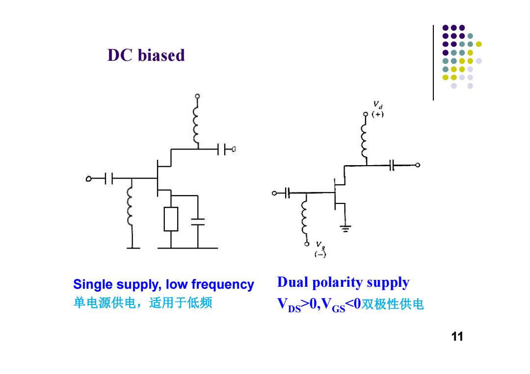
Single supply, low frequency 单电源供电,适用于低频 Dual polarity supply VDS>0,VGS<0双极性供电 DC biased 11