Analysis and Design of Analog Integrated Circuits UQSTC Analysis and Design of Analog Integrated Circuits (模拟集成电路分析与设计) 一进机 Instructor:Luo Ping 回 2019/9/3 UESTC Luo Ping
Analysis and Design of Analog Integrated Circuits 2019/9/3 UESTC Luo Ping 1 Analysis and Design of Analog Integrated Circuits (模拟集成电路分析与设计) Instructor: Luo Ping
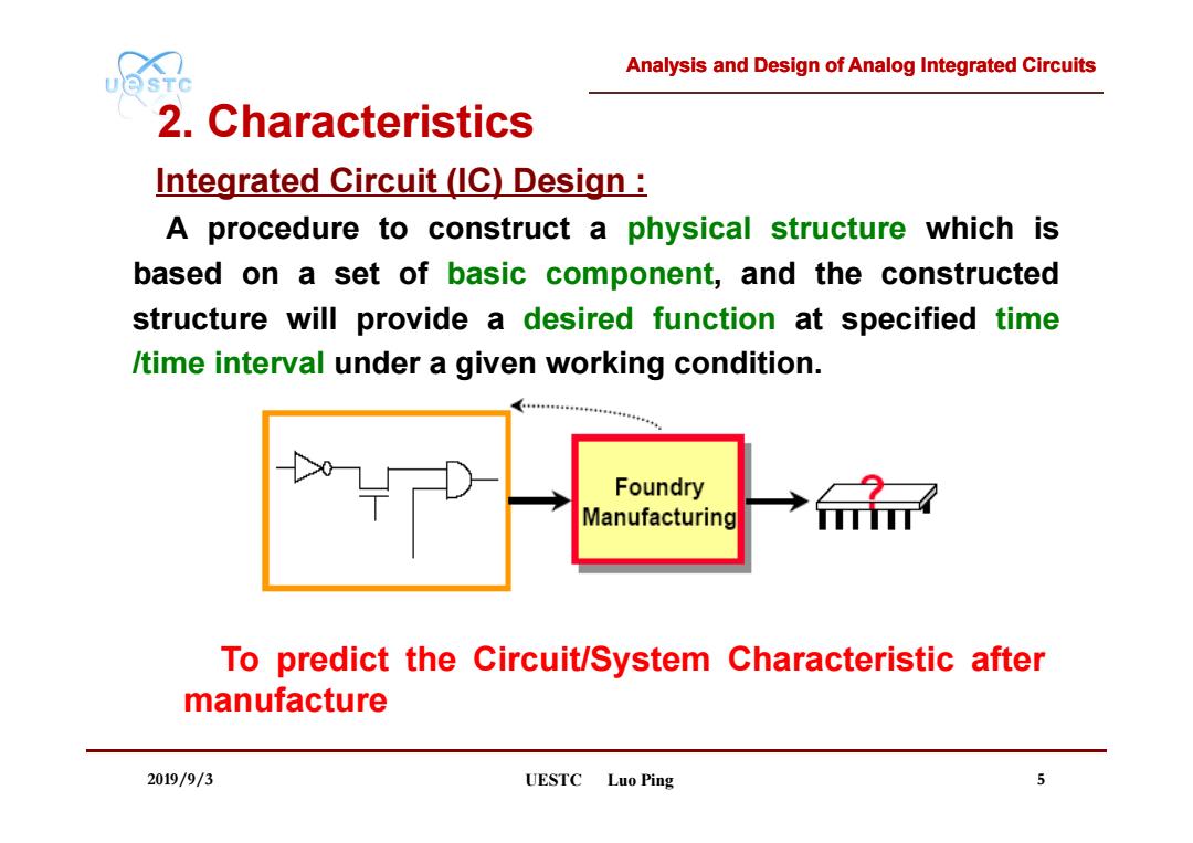
Analysis and Design of Analog Integrated Circuits UQSTC 2.Characteristics Integrated Circuit (IC)Design: A procedure to construct a physical structure which is based on a set of basic component,and the constructed structure will provide a desired function at specified time /time interval under a given working condition. Foundry Manufacturing To predict the Circuit/System Characteristic after manufacture 2019/9/3 UESTC Luo Ping 5
Analysis and Design of Analog Integrated Circuits 2019/9/3 UESTC Luo Ping 5 A procedure to construct a physical structure which is based on a set of basic component, and the constructed structure will provide a desired function at specified time /time interval under a given working condition. To predict the Circuit/System Characteristic after manufacture Integrated Circuit (IC) Design : 2. Characteristics
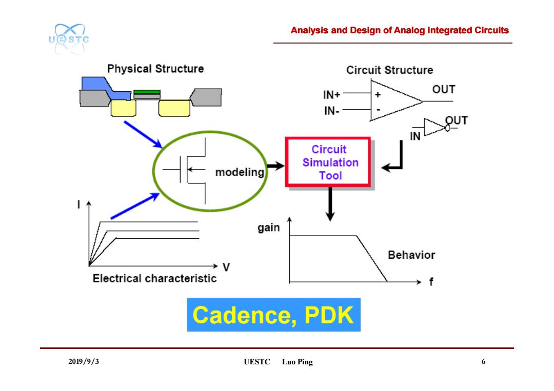
Analysis and Design of Analog Integrated Circuits UQSTC Physical Structure Circuit Structure IN+ OUT IN- UT Circuit Simulation modeling Tool gain Behavior →V Electrical characteristic Cadence,PDK 2019/9/3 UESTC Luo Ping 6
Analysis and Design of Analog Integrated Circuits 2019/9/3 UESTC Luo Ping 6 Cadence, PDK
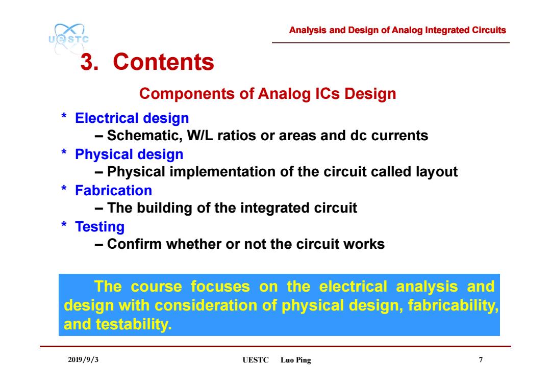
Analysis and Design of Analog Integrated Circuits 3.Contents Components of Analog ICs Design Electrical design Schematic,W/L ratios or areas and dc currents Physical design -Physical implementation of the circuit called layout Fabrication The building of the integrated circuit Testing Confirm whether or not the circuit works The course focuses on the electrical analysis and design with consideration of physical design,fabricability, and testability. 2019/9/3 UESTC Luo Ping
Analysis and Design of Analog Integrated Circuits 2019/9/3 UESTC Luo Ping 7 * Electrical design – Schematic, W/L ratios or areas and dc currents * Physical design – Physical implementation of the circuit called layout * Fabrication – The building of the integrated circuit * Testing – Confirm whether or not the circuit works 3. Contents Components of Analog ICs Design The course focuses on the electrical analysis and design with consideration of physical design, fabricability, and testability. The course focuses on the electrical analysis and design with consideration of physical design, fabricability, and testability
Analysis and Design of Analog Integrated Circuits UQSTC Chapter1 Models and comparison of integrated-circuit active devices --PN Junction --Large-Signal and Small-Signal Models of Bipolar Transistors -Large-Signal and Small-Signal Models of MOS Transistors --Comparison of BJT and MOS transistors 2019/9/3 UESTC Luo Ping 10
Analysis and Design of Analog Integrated Circuits 2019/9/3 UESTC Luo Ping 10 Chapter1 Models and comparison of integrated-circuit active devices -- PN Junction -- Large-Signal and Small-Signal Models of Bipolar Transistors -- Large-Signal and Small-Signal Models of MOS Transistors -- Comparison of BJT and MOS transistors
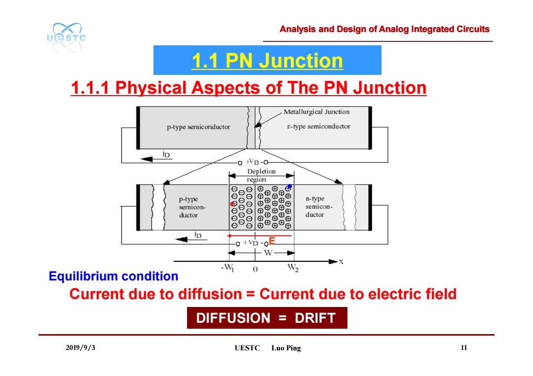
Analysis and Design of Analog Integrated Circuits UQSTC 1.1 PN Junction 1.1.1 Physical Aspects of The PN Junction Metallurgical Junction p-type semiconductor r-type semiconductor 0 4VD-0 Depletion region e p-type 9 的® 的 中 n-type semicon- semicon- ductor e 8 ⊙⊙ ⊕ ductor o & 由 母 D 0+D-o目 W -W 0 W2 Equilibrium condition Current due to diffusion Current due to electric field DIFFUSION DRIFT 2019/9/3 UESTC Luo Ping 11
Analysis and Design of Analog Integrated Circuits 2019/9/3 UESTC Luo Ping 11 1.1.1 Physical Aspects of The PN Junction E Current due to diffusion = Current due to electric field DIFFUSION = DRIFT Equilibrium condition 1.1 PN Junction
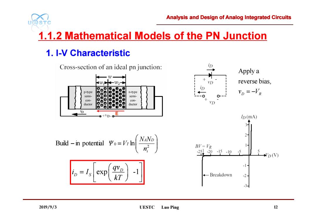
Analysis and Design of Analog Integrated Circuits UQSTC 1.1.2 Mathematical Models of the PN Junction 1.I-V Characteristic Cross-section of an ideal pn junction: D Apply a W1十Ww2 D reverse bias, p-type n-type Vp=-VR 0 semi- con- con- ductor 0 VD ⊙ ductor 0 D o+VD-0 Ip (mA) 2 NAND Build-in potential 平o=Vrh n BV=VR 1 220-5195 D(V) =Is exp -1 kT 4 Breakdown -2 3 2019/9/3 UESTC Luo Ping 12
Analysis and Design of Analog Integrated Circuits 2019/9/3 UESTC Luo Ping 12 1.1.2 Mathematical Models of the PN Junction 2 Build in potential 0 ln i A D T n N N Ψ V Apply a reverse bias, D R v V exp -1 D D S qv i I kT 1. I-V Characteristic E
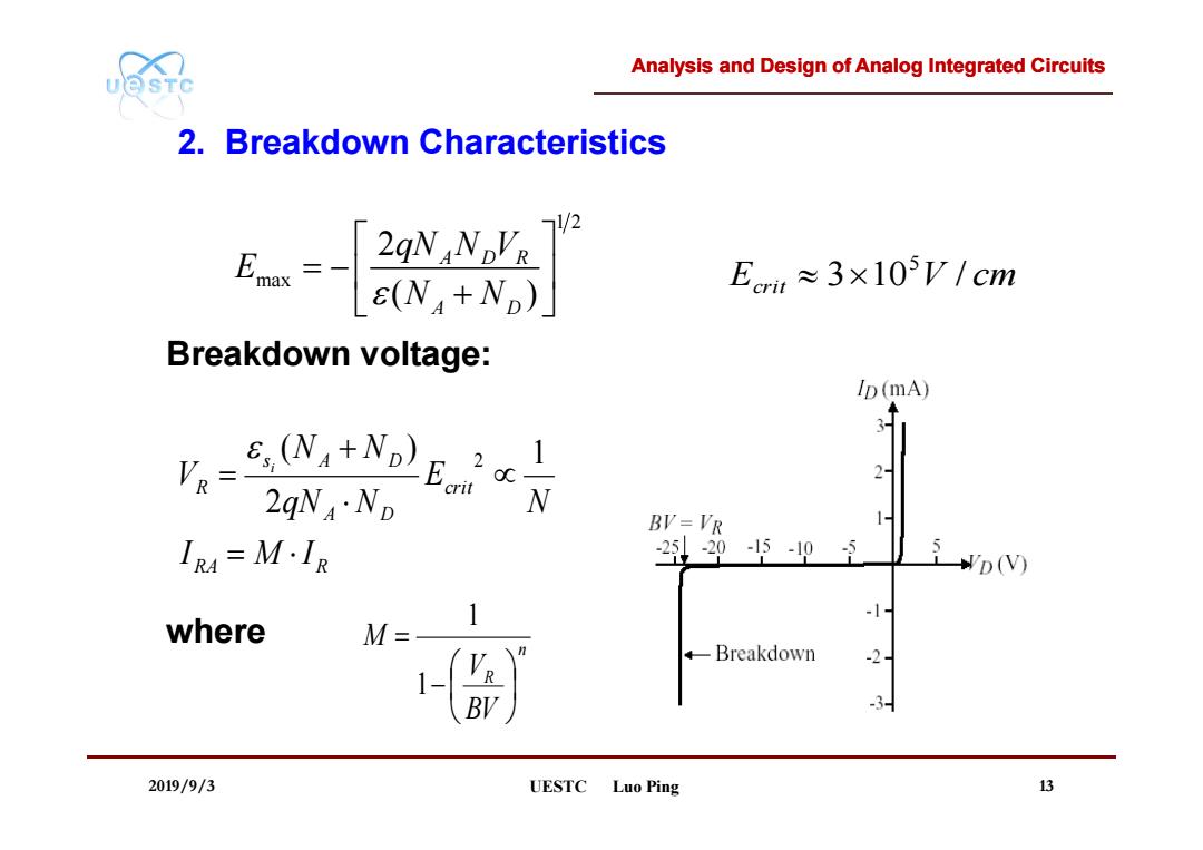
Analysis and Design of Analog Integrated Circuits UOSTC 2.Breakdown Characteristics 7/2 2qN NDVR E(N+Np) Em≈3×10⁵V/cm Breakdown voltage: Ip (mA) R=E NA+ND)E 3 2 2qN4·ND BV=VR IR4=M·IR 2205-95 D(V) 1 -1 where M= +Breakdown -2 BV 3 2019/9/3 UESTC Luo Ping 13
Analysis and Design of Analog Integrated Circuits 2019/9/3 UESTC Luo Ping 13 2. Breakdown Characteristics Breakdown voltage: where 1 2 max 2 ( ) A D R A D qN N V E N N RA R crit A D s A D R I M I N E qN N N N V i 1 2 ( ) 2 n R BV V M 1 1 Ecrit 3 10 V / cm 5
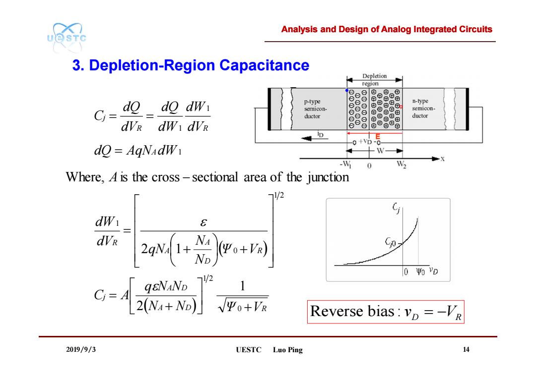
Analysis and Design of Analog Integrated Circuits UQSTC 3.Depletion-Region Capacitance Depletion region 8888 p-type n-type C= dodo dw semicon- ⊙⊙ semicon- ductor ductor dvr dw dvR D e 0+VD- do AgNadW -W 0 W2 Where,A is the cross-sectional area of the junction /2 E dVR 2o+岩+同 0 Yo YD qeNaND C-4 72 2WM+No]Vo+ Reverse bias:vp =-VR 2019/9/3 UESTC Luo Ping 14
Analysis and Design of Analog Integrated Circuits 2019/9/3 UESTC Luo Ping 14 A D R A D j R D A A R A R R j N N Ψ V q N N C A Ψ V N N qN dV dW A dQ AqN dW dV dW dW dQ dV dQ C 0 1 2 1 2 0 1 1 1 1 1 2 2 1 Where, is the cross sectional area of the junction 3. Depletion-Region Capacitance Reverse bias : D R v V
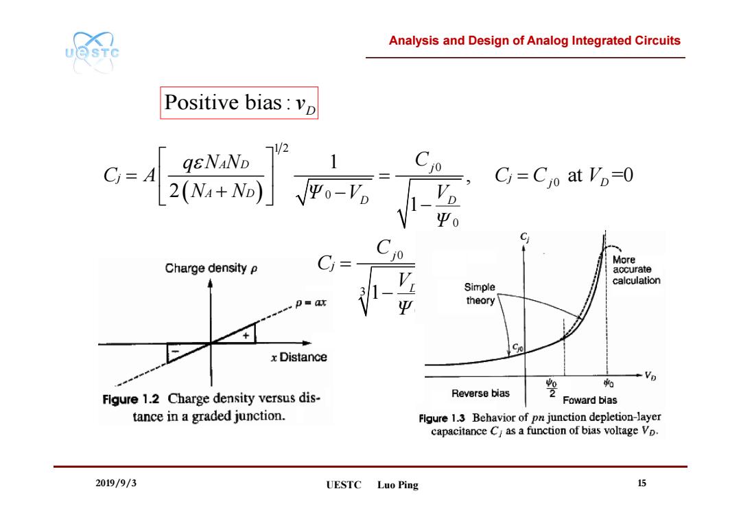
Analysis and Design of Analog Integrated Circuits UQSTC Positive bias:vp C=Cjo at Vp=0 Ψ0 C More Charge density P Ci= accurate Simple calculation p=ax Ψ theory 90 xDistance % Figure 1.2 Charge density versus dis- Reverse bias 2 Foward blas tance in a graded junction. Flgure 1.3 Behavior of pn junction depletion-layer capacitance Ci as a function of bias voltage Vp. 2019/9/3 UESTC Luo Ping 15
Analysis and Design of Analog Integrated Circuits 2019/9/3 UESTC Luo Ping 15 1 2 0 0 0 0 1 , at =0 2 1 A D j j j j D A D D D q N N C C A C C V N N Ψ V V Ψ Positive bias : Dv 0 3 0 1 j j D C C V Ψ