Chapter 10 Manipulating(处理),Computing,and Compensation(补偿)Devices by Yixin Ma 22/05/2013 Contents 2/26 1.Bridge Circuits 2.Amplifiers 3.Filters 4.Mathematic Operations: Integration and Differentiation Addition and Subtraction Multiplication and Division 5.Function Generation and Linearization 6.Amplitude Modulation and Demodulation 7.Voltage-to-frequency and Frequency-to-Voltage Converters 8.ADC and DAC;SHA
Chapter 10 Manipulating(处理), Computing, and Compensation(补偿) Devices by Yixin Ma 22/05/2013 Contents 1. Bridge Circuits 2. Amplifiers 3. Filters 4. Mathematic Operations: z Integration and Differentiation z Addition and Subtraction z Multiplication and Division 5. Function Generation and Linearization 6. Amplitude Modulation and Demodulation 7. Voltage-to-frequency and Frequency-to-Voltage Converters 8. ADC and DAC; SHA 2/26
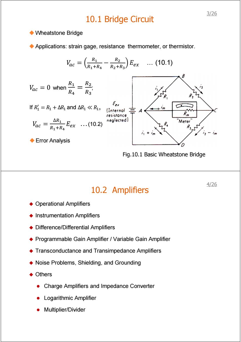
3/26 10.1 Bridge Circuit ◆Wheatstone Bridge Applications:strain gage,resistance thermometer,or thermistor. Vac= R1 )Eex(10.1) R1+R4R2+R3 Vac =0 when =2 R4 R3' Eer fR=R+AR and△R《R,(Interol m A AA resistance △R2Eex(10.2) Vac=R+R neglected R "Meter i+im 12-Im ◆Error Analysis D Fig.10.1 Basic Wheatstone Bridge 426 10.2 Amplifiers Operational Amplifiers Instrumentation Amplifiers Difference/Differential Amplifiers Programmable Gain Amplifier /Variable Gain Amplifier Transconductance and Transimpedance Amplifiers Noise Problems,Shielding,and Grounding ◆Others Charge Amplifiers and Impedance Converter Logarithmic Amplifier ●Multiplier/Divider
10.1 Bridge Circuit Fig.10.1 Basic Wheatstone Bridge Wheatstone Bridge Applications: strain gage, resistance thermometer, or thermistor. ܸ = ோభ ோభାோర − ோమ ோమାோయ ܧ௫ … (10.1) ܸ = 0 when ோభ ோర ோమ ோయ ; If ܴଵ ᇱ = ܴଵ + ∆ܴଵ and ∆ܴଵ ≪ ܴଵ, ܸ = ∆ோభ ோభାோర ܧ௫ …(10.2) Error Analysis 3/26 10.2 Amplifiers Operational Amplifiers Instrumentation Amplifiers Difference/Differential Amplifiers Programmable Gain Amplifier / Variable Gain Amplifier Transconductance and Transimpedance Amplifiers Noise Problems, Shielding, and Grounding Others z Charge Amplifiers and Impedance Converter z Logarithmic Amplifier z Multiplier/Divider 4/26
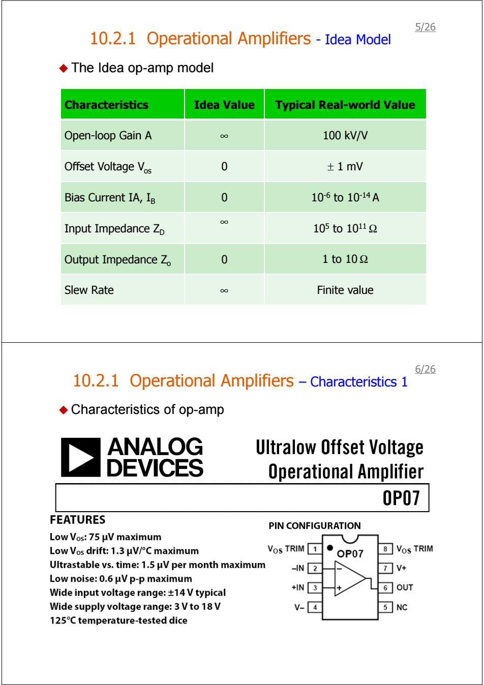
5/26 10.2.1 Operational Amplifiers-Idea Model ◆The Idea op-amp model Characteristics Idea Value Typical Real-world Value Open-loop Gain A 100 kV/V Offset Voltage Vos 0 ±1mv Bias Current IA,IB 0 106to10-14A Input Impedance Zp 105to10112 Output Impedance Zo 0 1to102 Slew Rate Finite value 6126 10.2.1 Operational Amplifiers-Characteristics 1 Characteristics of op-amp ANALOG Ultralow Offset Voltage DEVICES Operational Amplifier 0P07 FEATURES PIN CONFIGURATION Low Vos::75μVmaximum Low Vos drift:1.3μV/°C maximum Vos TRIM1 ● OP07 8☐Vos TRIM Ultrastable vs.time:1.5 uV per month maximum -N2 7☑V+ Low noise:0.6 uV p-p maximum Wide input voltage range:+14 V typical 6OUT Wide supply voltage range:3 Vto 18V v-4 5 NC 125C temperature-tested dice
10.2.1 Operational Amplifiers - Idea Model The Idea op-amp model Characteristics Idea Value Typical Real-world Value Open-loop Gain A ∞ 100 kV/V Offset Voltage Vos 0 ± 1 mV Bias Current IA, IB 0 10-6 to 10-14 A Input Impedance ZD ∞ 105 to 1011 Ω Output Impedance Zo 0 1 to 10 Ω Slew Rate ∞ Finite value 5/26 10.2.1 Operational Amplifiers – Characteristics 1 Characteristics of op-amp 6/26
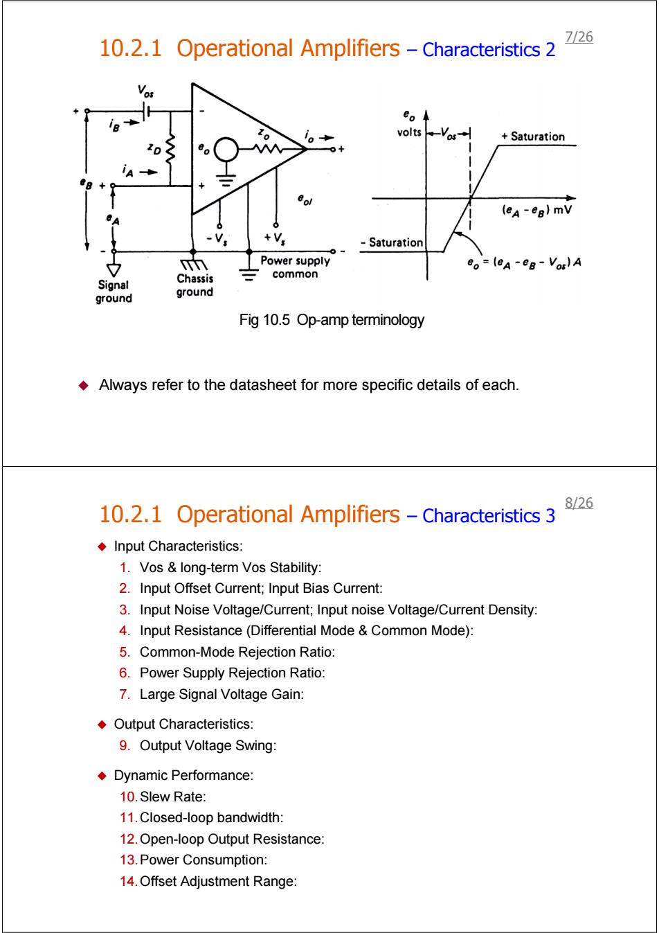
10.2.1 Operational Amplifiers-Characteristics 2 7/26 e。 voltsVas Saturation eol (ea-eg)mV -Saturation 中 Power supply eo=(eA-eB-Vos)A common Signal Chassis ground ground Fig 10.5 Op-amp terminology Always refer to the datasheet for more specific details of each. 8/26 10.2.1 Operational Amplifiers-Characteristics 3 Input Characteristics: 1.Vos long-term Vos Stability: 2.Input Offset Current;Input Bias Current: 3.Input Noise Voltage/Current;Input noise Voltage/Current Density: 4.Input Resistance(Differential Mode Common Mode): 5.Common-Mode Rejection Ratio: 6.Power Supply Rejection Ratio: 7.Large Signal Voltage Gain: Output Characteristics: 9.Output Voltage Swing: Dynamic Performance: 10.Slew Rate: 11.Closed-loop bandwidth: 12.Open-loop Output Resistance: 13.Power Consumption: 14.Offset Adjustment Range:
Always refer to the datasheet for more specific details of each. 10.2.1 Operational Amplifiers – Characteristics 2 Fig 10.5 Op-amp terminology 7/26 10.2.1 Operational Amplifiers – Characteristics 3 Input Characteristics: 1. Vos & long-term Vos Stability: 2. Input Offset Current; Input Bias Current: 3. Input Noise Voltage/Current; Input noise Voltage/Current Density: 4. Input Resistance (Differential Mode & Common Mode): 5. Common-Mode Rejection Ratio: 6. Power Supply Rejection Ratio: 7. Large Signal Voltage Gain: Output Characteristics: 9. Output Voltage Swing: Dynamic Performance: 10.Slew Rate: 11.Closed-loop bandwidth: 12.Open-loop Output Resistance: 13.Power Consumption: 14.Offset Adjustment Range: 8/26
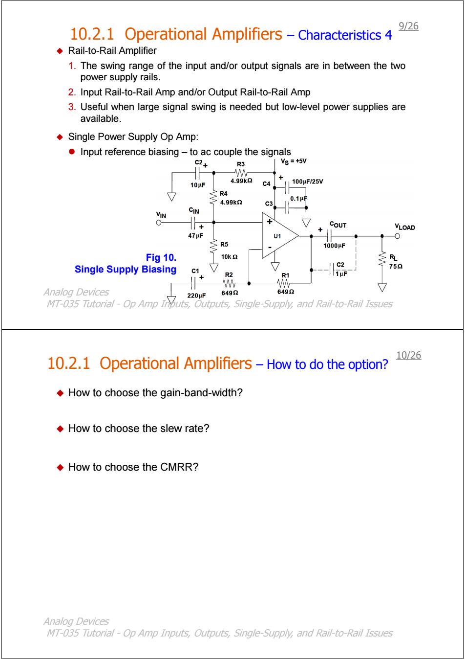
9/26 10.2.1 Operational Amplifiers -Characteristics 4 Rail-to-Rail Amplifier 1.The swing range of the input and/or output signals are in between the two power supply rails. 2.Input Rail-to-Rail Amp and/or Output Rail-to-Rail Amp 3.Useful when large signal swing is needed but low-level power supplies are available. Single Power Supply Op Amp: Input reference biasing-to ac couple the signals R3 Vs =+5V 10μF 4.99kn C4 1100μF/25V 之R4 4.99k2 0.1μ c3 CIN COUT VLOAD 47μF U1 0 三R5 1000μF Fig 10. 10k2 RL Single Supply Biasing C2 75Ω C1 R2 R1 1μF Analog Devices 6492 6492 220μF MT-035 Tutorial-Op Amp Inouts,Outputs,Single-Supply,and Rail-to-Rail Issues 10/26 10.2.1 Operational Amplifiers-How to do the option? How to choose the gain-band-width? How to choose the slew rate? How to choose the CMRR? Analog Devices MT-035 Tutorial-Op Amp Inputs,Outputs,Single-Supply,and Rail-to-Rail Issues
10.2.1 Operational Amplifiers – Characteristics 4 Rail-to-Rail Amplifier 1. The swing range of the input and/or output signals are in between the two power supply rails. 2. Input Rail-to-Rail Amp and/or Output Rail-to-Rail Amp 3. Useful when large signal swing is needed but low-level power supplies are available. Single Power Supply Op Amp: z Input reference biasing – to ac couple the signals Fig 10. Single Supply Biasing Analog Devices MT-035 Tutorial - Op Amp Inputs, Outputs, Single-Supply, and Rail-to-Rail Issues 9/26 10.2.1 Operational Amplifiers – How to do the option? How to choose the gain-band-width? How to choose the slew rate? How to choose the CMRR? Analog Devices MT-035 Tutorial - Op Amp Inputs, Outputs, Single-Supply, and Rail-to-Rail Issues 10/26
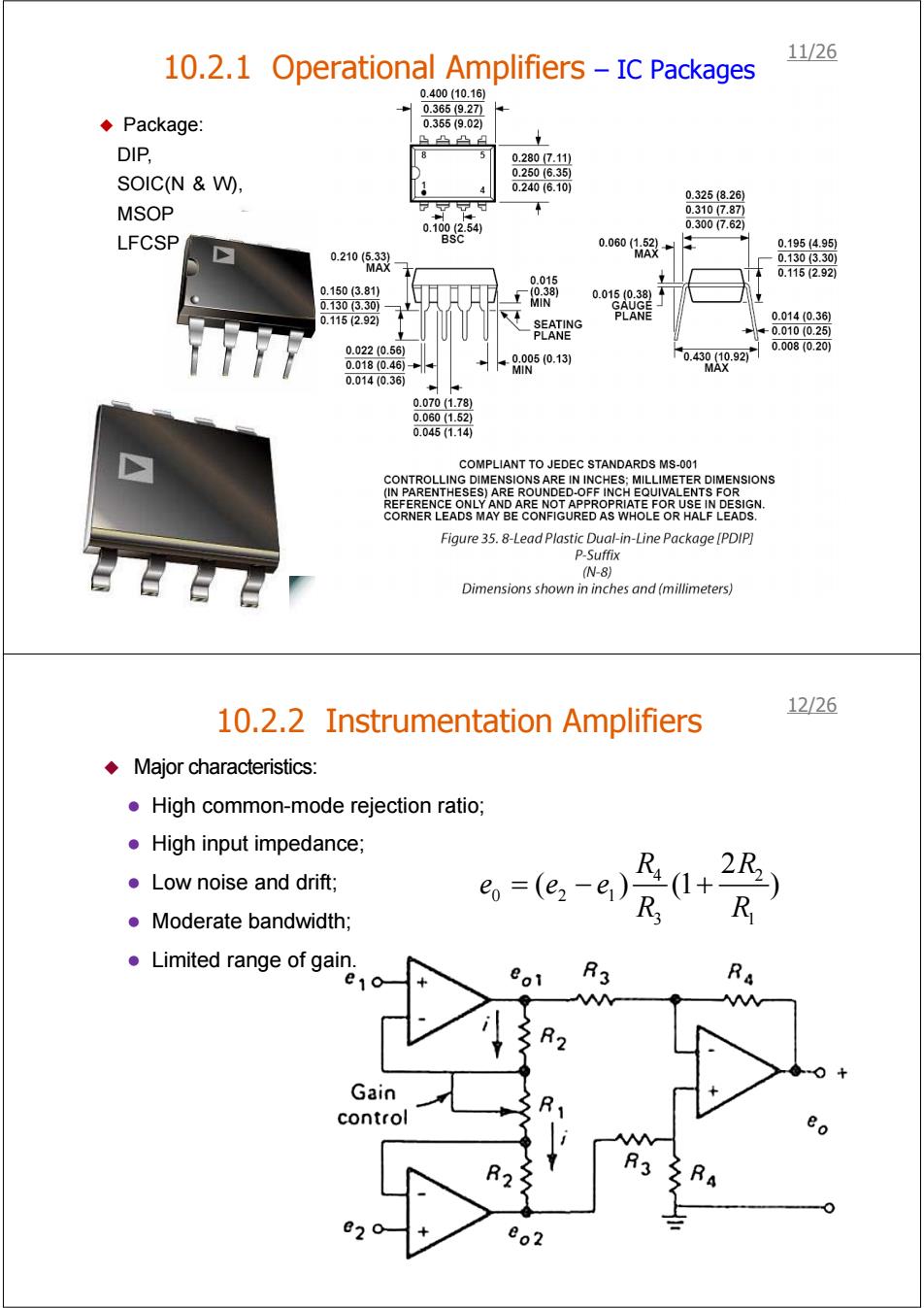
11/26 10.2.1 Operational Amplifiers-IC Packages 0.400(10.16) 0.365(9.27) 人 ◆Package: 0.355(9.02) 凸凸凸 DIP, 0.280(7.11) 0.250(6.35) SOIC(N W), 0.240(6.10) 0.325(8.26) MSOP 0.310(7.87 0.100(2.54) 0.300(7.62) LFCSP BSC 0.195(4.95) 0.210(5.33) 00601殷 0.130(3.30) MAX 0.015 0.1152.92) 0.150(3.81) 0.38) 0.015(0.38) 0.1303.30) MIN GAUGE 0.115(2.92 SEATING PLANE 0.014(0.36) PLANE +0.010(0.25) 0.022(0.56) 0.018(0.46)+ 0.005(0.13) 0.430(10.92 0.008(0.201 MIN MAX 0.014(0.36) 0.070(1.78) 0.060(1.52 0.045(1.14) COMPLIANT TO JEDEC STANDARDS MS-001 CONTROLLING DIMENSIONS ARE IN INCHES:MILLIMETER DIMENSIONS 腔aE5思9RRE8 APPROPRIATE FOR USE IN D8icN. CORNER LEADS MAY BE CONFIGURED AS WHOLE OR HALF LEADS. Figure 35.8-Lead Plastic Dual-in-Line Package [PDIP] P-Suffix (N-8) Dimensions shown in inches and(millimeters) 12/26 10.2.2 Instrumentation Amplifiers Major characteristics: High common-mode rejection ratio; High input impedance; ●Low noise and drift;: eo=(ez-4)R 2R2 R ●Moderate bandwidth; Limited range of gain. R3 Gain control
Package: DIP, SOIC(N & W), MSOP LFCSP 10.2.1 Operational Amplifiers – IC Packages 11/26 4 2 0 21 3 1 2 ( ) (1 ) R R e ee R R =− + 10.2.2 Instrumentation Amplifiers 12/26 Major characteristics: z High common-mode rejection ratio; z High input impedance; z Low noise and drift; z Moderate bandwidth; z Limited range of gain
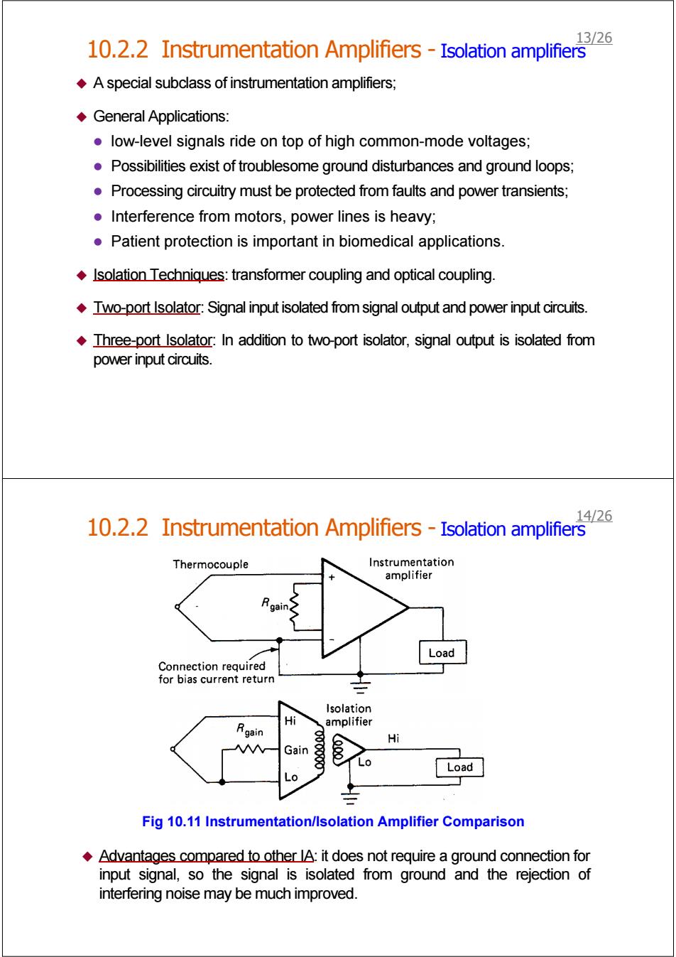
3/26 10.2.2 Instrumentation Amplifiers -Isolation amplifiers A special subclass of instrumentation amplifiers; General Applications: low-level signals ride on top of high common-mode voltages; Possibilities exist of troublesome ground disturbances and ground loops; Processing circuitry must be protected from faults and power transients; Interference from motors,power lines is heavy; Patient protection is important in biomedical applications. Isolation Techniques:transformer coupling and optical coupling. Two-port Isolator:Signal input isolated from signal output and power input circuits. Three-port Isolator:In addition to two-port isolator,signal output is isolated from power input circuits. 4/26 10.2.2 Instrumentation Amplifiers-Isolation amplifiers Thermocouple Instrumentation amplifier Load Connection required for bias current return Isolation Hi amplifier Hi Gain Lo Load Fig 10.11 Instrumentation/lsolation Amplifier Comparison Advantages compared to other IA:it does not require a ground connection for input signal,so the signal is isolated from ground and the rejection of interfering noise may be much improved
A special subclass of instrumentation amplifiers; General Applications: z low-level signals ride on top of high common-mode voltages; z Possibilities exist of troublesome ground disturbances and ground loops; z Processing circuitry must be protected from faults and power transients; z Interference from motors, power lines is heavy; z Patient protection is important in biomedical applications. Isolation Techniques: transformer coupling and optical coupling. Two-port Isolator: Signal input isolated from signal output and power input circuits. Three-port Isolator: In addition to two-port isolator, signal output is isolated from power input circuits. 10.2.2 Instrumentation Amplifiers - Isolation amplifiers13/26 Fig 10.11 Instrumentation/Isolation Amplifier Comparison Advantages compared to other IA: it does not require a ground connection for input signal, so the signal is isolated from ground and the rejection of interfering noise may be much improved. 10.2.2 Instrumentation Amplifiers - Isolation amplifiers14/26
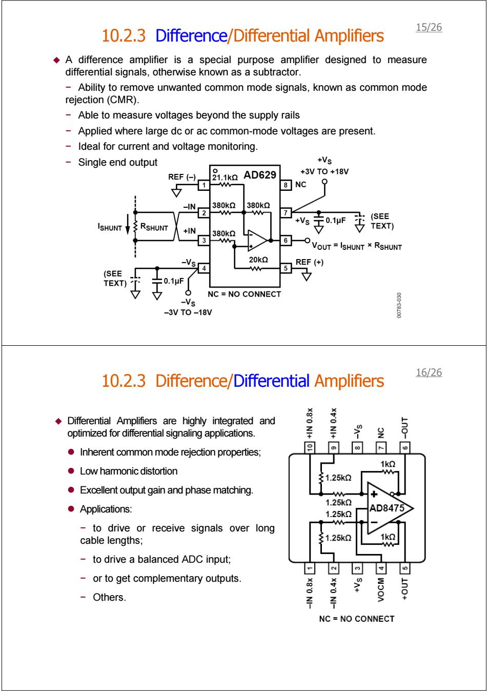
10.2.3 Difference/Differential Amplifiers 15/26 A difference amplifier is a special purpose amplifier designed to measure differential signals,otherwise known as a subtractor. Ability to remove unwanted common mode signals,known as common mode rejection(CMR). Able to measure voltages beyond the supply rails Applied where large dc or ac common-mode voltages are present. Ideal for current and voltage monitoring. Single end output +Vs 21.1kaAD629 +3VT0+18V REF (- 5 1 M 8NC -IN 380kQ 380kQ 2 w 7 +Vs左0.1F (SEE ISHUNT RSHUNT TEXT) +IN 380kQ 3 6VOUT=ISHUNT RSHUNT 20kQ (SEE 包g” TEXT) 0.1μf NC NO CONNECT -Vs -3V TO-18V 16/26 10.2.3 Difference/Differential Amplifiers 的 Differential Amplifiers are highly integrated and optimized for differential signaling applications. ” Inherent common mode rejection properties; 1k2 Low harmonic distortion 1.25k2 Excellent output gain and phase matching. 1.25k ●Applications: AD8475> 1.25k2 to drive or receive signals over long w cable lengths; 1.25k 1k2 to drive a balanced ADC input; or to get complementary outputs. Others. NC NO CONNECT
A difference amplifier is a special purpose amplifier designed to measure differential signals, otherwise known as a subtractor. − Ability to remove unwanted common mode signals, known as common mode rejection (CMR). − Able to measure voltages beyond the supply rails − Applied where large dc or ac common-mode voltages are present. − Ideal for current and voltage monitoring. − Single end output 10.2.3 Difference/Differential Amplifiers 15/26 Differential Amplifiers are highly integrated and optimized for differential signaling applications. z Inherent common mode rejection properties; z Low harmonic distortion z Excellent output gain and phase matching. z Applications: − to drive or receive signals over long cable lengths; − to drive a balanced ADC input; − or to get complementary outputs. − Others. 10.2.3 Difference/Differential Amplifiers 16/26
17/26 10.2.4 PGA VGA A Programmable Gain Instrumentation Amplifier (PGiA,PGA)is a special form of in-amp that has DGND WR A1 fixed gain levels. 26 LOGIC The appropriate gain level is selected by digital means,either by dedicated program pins,or by software interfaces(SPI or 12C). The PGiAs are perfect for those applications where gain accuracy must be maximized,or where a single PGiA can take the place of +IN 10 AD8253 several in-amps of different gain settings. +Vs 9 +Vs AD8253 AD8253 REF 1 R fHIGH-PASS =2TTRC AD8253 10M2 REF -Vs THERMOCOUPLE -Vs TRANSFORMER Vs 10.2.4 PGA VGA 1826 ◆hat are VGAs? -Variable gain amplifiers (VGAs)are signal-conditioning amplifiers with electronically settable voltage gain. There are analog VGAs and digital VGAs,or DVGAs. A digital-to-analog converter(DAC),a functional source,or a dc source can provide the analog voltage control. Ultrasound scanners and phased-array radars favor analog VGAs.They both involve a massive number of parallel amplifiers that all require a common gain control. A cable TV system in which the level of the upstream signal from the consumer's set-top box is adjusted for cable attenuation by a downstream signal from the cable company's head-end.This would be a case for a digital VGA. PRAO VGAI VGAs are available from dc to gigahertz frequencies ATTENUATOR PrA -60dB TO 0dB 1 VOUT and in a variety of 1/O INPN(5 AD8336 configurations. Relative low CMRR BIAS GAIN CONTROL compared to PGiA INTERFACE .10 13 3 11 12 NEG VPOS VCOM GPOS GNEG
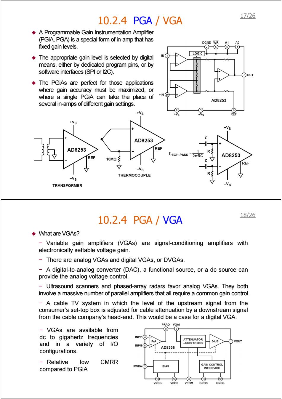
10.2.4 PGA / VGA A Programmable Gain Instrumentation Amplifier (PGiA, PGA) is a special form of in-amp that has fixed gain levels. The appropriate gain level is selected by digital means, either by dedicated program pins, or by software interfaces (SPI or I2C). The PGiAs are perfect for those applications where gain accuracy must be maximized, or where a single PGiA can take the place of several in-amps of different gain settings. 17/26 What are VGAs? − Variable gain amplifiers (VGAs) are signal-conditioning amplifiers with electronically settable voltage gain. − There are analog VGAs and digital VGAs, or DVGAs. − A digital-to-analog converter (DAC), a functional source, or a dc source can provide the analog voltage control. − Ultrasound scanners and phased-array radars favor analog VGAs. They both involve a massive number of parallel amplifiers that all require a common gain control. − A cable TV system in which the level of the upstream signal from the consumer’s set-top box is adjusted for cable attenuation by a downstream signal from the cable company’s head-end. This would be a case for a digital VGA. 10.2.4 PGA / VGA − VGAs are available from dc to gigahertz frequencies and in a variety of I/O configurations. − Relative low CMRR compared to PGiA 18/26
9/26 10.2.5 Transconductance and Transimpedance Amplifiers When the input is a voltage and the output is a current,the amplifier is called transconductance whereas the reverse situation is called transimpedance. 60 MHz 2000 V/us ◆Transconductance: Monolithic Op Amp AD844 -A single-chip solution for converting voltage into a current output,can be used as voltage controlled current source. Ground Base ● ● 9 ◆Transimpedance: 2o Emitter -A single-chip solution for converting control Switching Stage photodiode current into a differential OTA voltage output,supporting data rates from Sampling Comparator(SC) 12Collector 155Mbps to 11.1Gbps. (louT) -Fiber Optic Transimpedance Amplifiers o19 SOTA Biasing S/H 11 O lo Adjust Photo Detector with integrated loss of In- signal (LOS)detection circuitry. OPA615 13 5 cc cc 20/26 10.2.6 Noise Problems,Shielding,and Grounding Amplifier drifts can be controlled when line voltage and temperature are kept constant. Inductive pickup (via magnetic field),electrostatic pickup (via stray capacitance),and ground loops can cause large error voltages,often concentrated at the power-line frequency. ◆Solutions: Remove interfering devices (power lines,motors,transformers,fluorescent() lamps,relays,etc.)from the near field of sensitive signal circuits. Use of an enclosing conductive shield as shown in Fig.10.13.The captured charges in she shield must be drained off to a satisfactory ground. Electrostatic source Use twisted pair of conductors to reduce the pick up of low frequency magnetically induce noise. Source-to-shield capacitance Signal conductors -Shield Fig.10.13 Electrostatic Shielding Shield-to-cable Ground capacitance
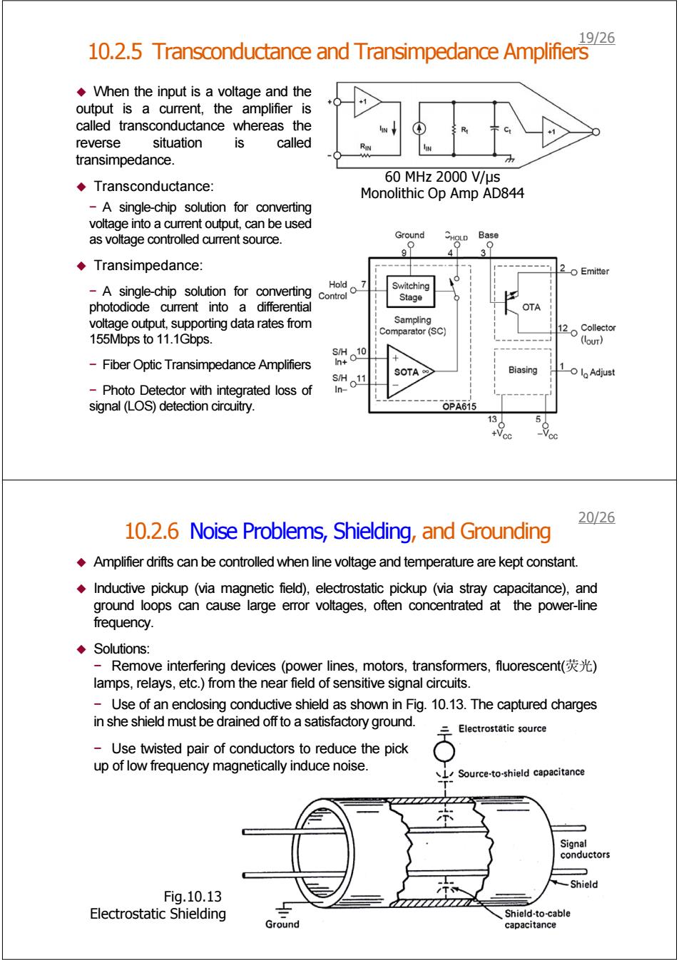
When the input is a voltage and the output is a current, the amplifier is called transconductance whereas the reverse situation is called transimpedance. Transconductance: − A single-chip solution for converting voltage into a current output, can be used as voltage controlled current source. Transimpedance: − A single-chip solution for converting photodiode current into a differential voltage output, supporting data rates from 155Mbps to 11.1Gbps. − Fiber Optic Transimpedance Amplifiers − Photo Detector with integrated loss of signal (LOS) detection circuitry. 10.2.5 Transconductance and Transimpedance Amplifiers 60 MHz 2000 V/μs Monolithic Op Amp AD844 19/26 Amplifier drifts can be controlled when line voltage and temperature are kept constant. Inductive pickup (via magnetic field), electrostatic pickup (via stray capacitance), and ground loops can cause large error voltages, often concentrated at the power-line frequency. Solutions: − Remove interfering devices (power lines, motors, transformers, fluorescent(荧光) lamps, relays, etc.) from the near field of sensitive signal circuits. − Use of an enclosing conductive shield as shown in Fig. 10.13. The captured charges in she shield must be drained off to a satisfactory ground. 10.2.6 Noise Problems, Shielding, and Grounding Fig.10.13 Electrostatic Shielding − Use twisted pair of conductors to reduce the pick up of low frequency magnetically induce noise. 20/26