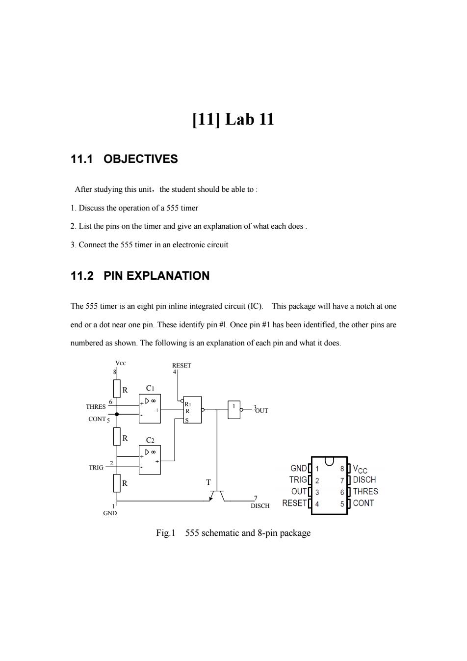
[11]Lab11 11.1 OBJECTIVES After studying this unit,the student should be able to: 1.Discuss the operation of a 555 timer 2.List the pins on the timer and give an explanation of what each does. 3.Connect the 555 timer in an electronic circuit 11.2 PIN EXPLANATION The 555 timer is an eight pin inline integrated circuit(IC).This package will have a notch at one end or a dot near one pin.These identify pin #l.Once pin #1 has been identified,the other pins are numbered as shown.The following is an explanation of each pin and what it does. Vcc RESET R THRES OUT CONT5 >o0 TRIG-2 GNDI 1 8 Vcc R T TRIG > DISCH OUTI 3 6 THRES 7 DISCH RESETn 4 5 CONT GND Fig.1 555 schematic and 8-pin package
[11] Lab 11 11.1 OBJECTIVES After studying this unit,the student should be able to : 1. Discuss the operation of a 555 timer 2. List the pins on the timer and give an explanation of what each does . 3. Connect the 555 timer in an electronic circuit 11.2 PIN EXPLANATION The 555 timer is an eight pin inline integrated circuit (IC). This package will have a notch at one end or a dot near one pin. These identify pin #l. Once pin #1 has been identified, the other pins are numbered as shown. The following is an explanation of each pin and what it does. R 1 1 R S RESET 4 3 OUT VCC 8 6 THRES CONT 5 2 TRIG 1 GND 7 DISCH + - + + - + T C1 C2 R R R Fig.1 555 schematic and 8-pin package

0 0 0 0 G 0 0 Fig RS Latch Pin #1 Ground This pin is connected to circuit ground. Pin#2 Trigger This pin must be connected to a voltage which is less than one-third Vcc (the applied voltage)to trigger the unit.This is general done by connecting pin #2 to ground. The connection to one-third Vcc or ground must be momentary.If pin #2 is not removed from ground the unit will not operate. Pin#3 Output The output turns on when pin#2 is triggered,and off when the discharge is turned on. Pin#4 Reset When this pin is connected to Vcc it permits the unit to operate.When connected to ground it activates the discharge and keeps the timer from operating. Pin#5 Control voltage If this pin is connected to Vcc through a variable resistor,the on time becomes longer.The off time remains unaffected.If it is connected to ground through a variable resistor,the on time becomes shorter.The off time is still not affected.If it is not used in the circuit,it is generally taken to ground through a small capacitor.This prevents circuit noise from talking to pin #5. Pin#6 Threshold When the voltage across the capacitor connected to pin #6 reaches two-thirds of the value of Vcc. the discharge turns on and the output turns off. Pin#7 Discharge When pin #6 turns the discharge on,it discharges the capacitor connected to pin #6.The discharge remains turned on until pin #2 retriggers the timer.It then turns off and the capacitor
G1 G2 Q Q R S R S Q 0 0 Q 0 1 1 1 0 0 1 1 × Fig RS Latch Pin #1 Ground This pin is connected to circuit ground. Pin#2 Trigger This pin must be connected to a voltage which is less than one-third Vcc (the applied voltage) to trigger the unit. This is general done by connecting pin #2 to ground. The connection to one-third Vcc or ground must be momentary. If pin #2 is not removed from ground the unit will not operate. Pin#3 Output The output turns on when pin#2 is triggered, and off when the discharge is turned on. Pin#4 Reset When this pin is connected to Vcc it permits the unit to operate. When connected to ground it activates the discharge and keeps the timer from operating. Pin#5 Control voltage If this pin is connected to Vcc through a variable resistor, the on time becomes longer. The off time remains unaffected. If it is connected to ground through a variable resistor, the on time becomes shorter. The off time is still not affected. If it is not used in the circuit, it is generally taken to ground through a small capacitor. This prevents circuit noise from talking to pin #5. Pin#6 Threshold When the voltage across the capacitor connected to pin #6 reaches two-thirds of the value of Vcc, the discharge turns on and the output turns off. Pin#7 Discharge When pin #6 turns the discharge on, it discharges the capacitor connected to pin #6. The discharge remains turned on until pin #2 retriggers the timer. It then turns off and the capacitor
connected to pin #6 begins charging again. Pin #8 Vcc This pin is connected to the applied voltage of the circuit which is known as Vcc.The 555 timer operates on a wide range of voltages.Its operating voltage range is considered to be between 3 and 16 volts DC. (Note:For the following explanation,assume that pin #2 is connected to pin #6.This permits the unit to be retriggered by the discharge each time it turns on and discharges the capacitor to one-third the value of Vcc.) 11.3 OPERATION OF THE TIMER The 555 timer operates on a percentage of the applied voltage.The time setting remains constant even if the applied voltage changes.When the capacitor connected to pin #6 reaches two-third of the applied voltage,the discharge turns on.The capacitor discharges until it reaches one-third of the applied voltage.If Vcc of the timer is connected to 12 volts DC,two-thirds of the applied voltage is 8 volts and one-third is 4 volts.This means that when the voltage across the capacitor connected to pin #6 reaches 8 volts,pin #7 turns on.After the capacitor discharges to one-third the value of Vcc,or 4 volts,it turns off. If the voltage is lowered to 6 volts at Vcc,two-thirds of the applied voltage becomes 4 volts and one-third is 2 volts.Pin #7 now turns on when the voltage across the capacitor connected to pin #6 reaches 4 volts.It turns off when the voltage across the capacitor drops to 2 volts There is no mention of voltage in the formula.It takes just as long to charge the capacitor if the circuit is connected to 12 volts as it will for 6 volts.The voltage of the capacitor connected to pin #6 reaches two-thirds of Vcc the same way.When the timer has an applied voltage of 12 volts it takes the same amount of time as when the applied voltage is only 6 volts.Notice that the timing of the circuit remains the same even if the voltage changes
connected to pin #6 begins charging again. Pin #8 Vcc This pin is connected to the applied voltage of the circuit which is known as Vcc. The 555 timer operates on a wide range of voltages. Its operating voltage range is considered to be between 3 and 16 volts DC. (Note: For the following explanation, assume that pin #2 is connected to pin #6. This permits the unit to be retriggered by the discharge each time it turns on and discharges the capacitor to one-third the value of Vcc.) 11.3 OPERATION OF THE TIMER The 555 timer operates on a percentage of the applied voltage. The time setting remains constant even if the applied voltage changes. When the capacitor connected to pin #6 reaches two-third of the applied voltage, the discharge turns on. The capacitor discharges until it reaches one-third of the applied voltage. If Vcc of the timer is connected to 12 volts DC, two-thirds of the applied voltage is 8 volts and one-third is 4 volts. This means that when the voltage across the capacitor connected to pin #6 reaches 8 volts, pin #7 turns on .After the capacitor discharges to one-third the value of Vcc ,or 4 volts, it turns off. If the voltage is lowered to 6 volts at Vcc, two-thirds of the applied voltage becomes 4 volts and one-third is 2 volts. Pin #7 now turns on when the voltage across the capacitor connected to pin #6 reaches 4 volts. It turns off when the voltage across the capacitor drops to 2 volts. There is no mention of voltage in the formula. It takes just as long to charge the capacitor if the circuit is connected to 12 volts as it will for 6 volts. The voltage of the capacitor connected to pin #6 reaches two-thirds of Vcc the same way. When the timer has an applied voltage of 12 volts it takes the same amount of time as when the applied voltage is only 6 volts. Notice that the timing of the circuit remains the same even if the voltage changes
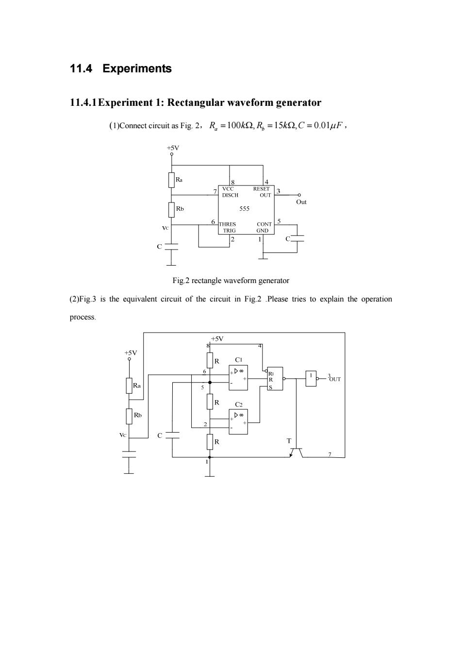
11.4 Experiments 11.4.1Experiment 1:Rectangular waveform generator (1)Connect circuit as Fig.2,R =100k,R =15k,C=0.01uF, +5V 8 4 RESET DISCH OUT Out Rb 555 6THRES CONT TRIG GND Fig.2 rectangle waveform generator (2)Fig.3 is the equivalent circuit of the circuit in Fig.2 Please tries to explain the operation process. +5V 8 R Ra T
11.4 Experiments 11.4.1Experiment 1: Rectangular waveform generator (1)Connect circuit as Fig. 2, 100 , 15 , 0.01 Ra b kR kC F , Fig.2 rectangle waveform generator (2)Fig.3 is the equivalent circuit of the circuit in Fig.2 .Please tries to explain the operation process
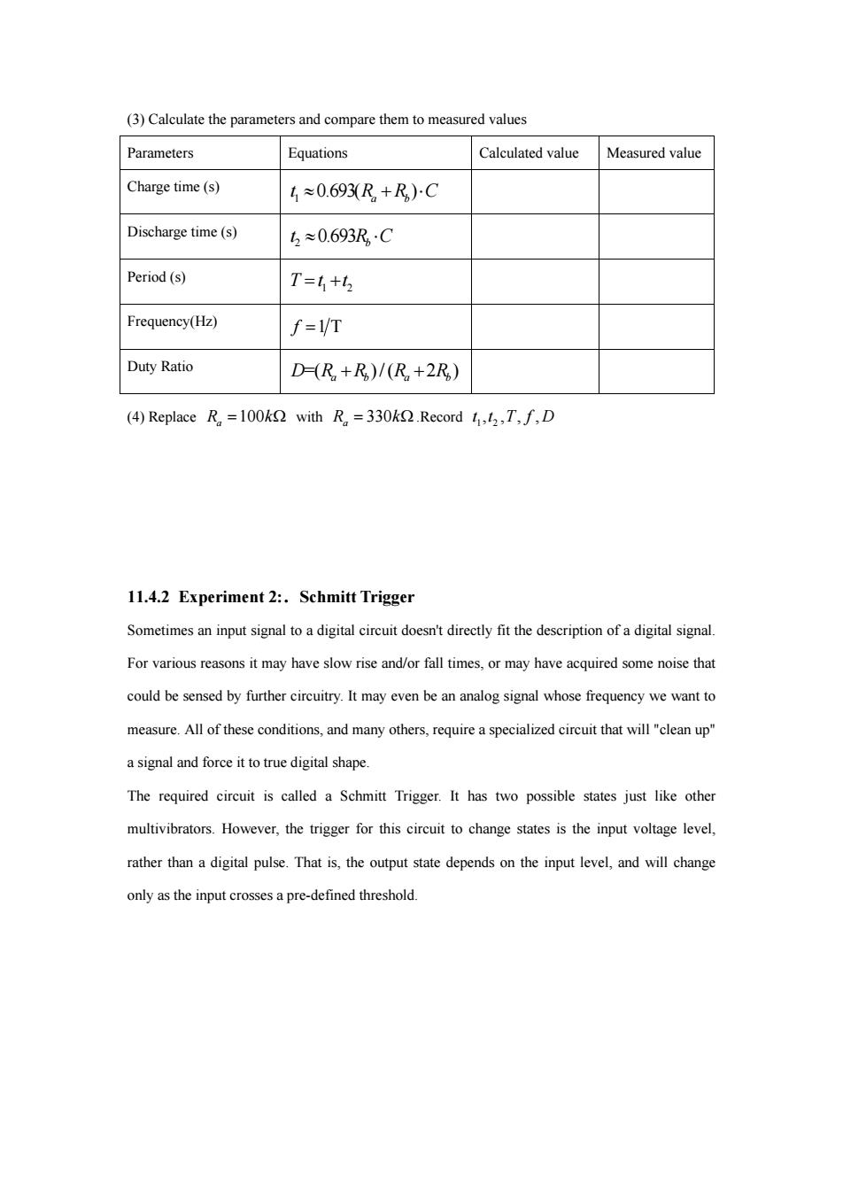
(3)Calculate the parameters and compare them to measured values Parameters Equations Calculated value Measured value Charge time(s) 4≈0.693R+R)C Discharge time(s) 5≈0.693R·C Period(s) T=4+h Frequency(Hz) f=1T Duty Ratio D(R+R)/(R+2R) (4)Replace R =100k with R.=330k2.Record t,,T,f,D 11.4.2 Experiment 2:.Schmitt Trigger Sometimes an input signal to a digital circuit doesn't directly fit the description of a digital signal. For various reasons it may have slow rise and/or fall times,or may have acquired some noise that could be sensed by further circuitry.It may even be an analog signal whose frequency we want to measure.All of these conditions,and many others,require a specialized circuit that will "clean up" a signal and force it to true digital shape. The required circuit is called a Schmitt Trigger.It has two possible states just like other multivibrators.However,the trigger for this circuit to change states is the input voltage level, rather than a digital pulse.That is,the output state depends on the input level,and will change only as the input crosses a pre-defined threshold
(3) Calculate the parameters and compare them to measured values Parameters Equations Calculated value Measured value Charge time (s) 1 0.693( ) a b t R RC Discharge time (s) 2 0.693 b t RC Period (s) Ttt 1 2 Frequency(Hz) f 1 T Duty Ratio =( ) / ( 2 ) DR R R R ab a b (4) Replace 100 Ra k with 330 Ra k.Record 1 2 tt TfD ,,,, 11.4.2 Experiment 2:.Schmitt Trigger Sometimes an input signal to a digital circuit doesn't directly fit the description of a digital signal. For various reasons it may have slow rise and/or fall times, or may have acquired some noise that could be sensed by further circuitry. It may even be an analog signal whose frequency we want to measure. All of these conditions, and many others, require a specialized circuit that will "clean up" a signal and force it to true digital shape. The required circuit is called a Schmitt Trigger. It has two possible states just like other multivibrators. However, the trigger for this circuit to change states is the input voltage level, rather than a digital pulse. That is, the output state depends on the input level, and will change only as the input crosses a pre-defined threshold

+5N。 Ra 4 8 RESET VCC THRES 3 Vo 555 OUT 8 2TRIG GND 1 Rb Fig.4 Schmitt Trigger (1)Connect circuit as Fig.4 R =100k,R =100k,C=0.1uF (2)Input sinusoidal signal,IkHz,peak to peak voltage is about V2V-31(3) measure the output signal by cursor function. Input signal:peao Output signal:V= Vlan
4 8 3 1 2 6 555 Ra Rb +5V C Vo Vi RESET OUT VCC THRES TRIG GND Fig. 4 Schmitt Trigger (1) Connect circuit as Fig.4 100 , 100 , 0.1 Ra b kR kC F (2) Input sinusoidal signal, 1kHz, peak to peak voltage is about 2 3 V VV peak to peak (3) measure the output signal by cursor function. Input signal: Vpeak to peak Vrms Output signal: Vhigh Vlow
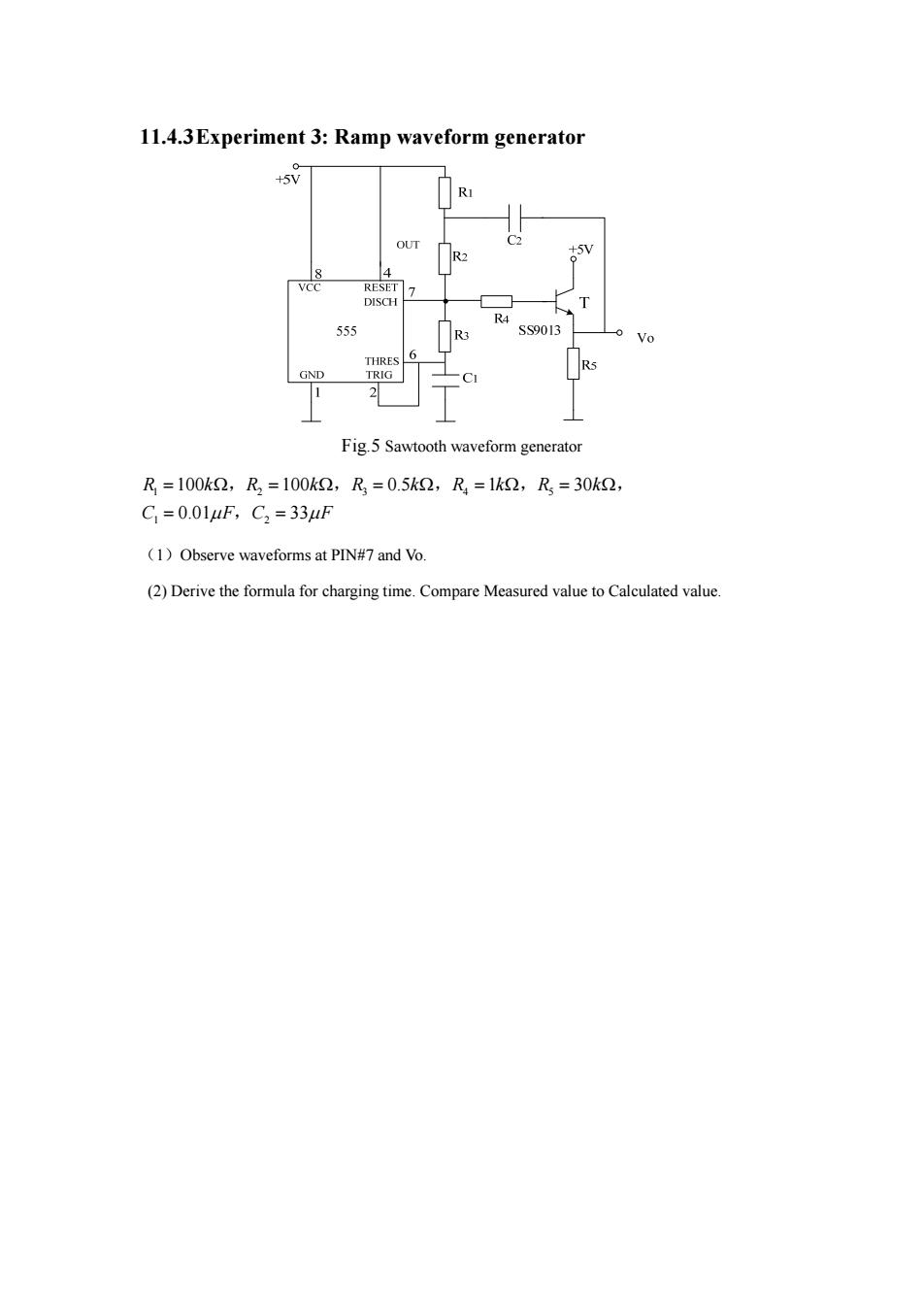
11.4.3Experiment 3:Ramp waveform generator +5V OUT R2 +5V 4 VCC RESET 7 DISCH 心 555 R3 SS9013 Vo THRES 6 GND TRIG 2 Fig.5 Sawtooth waveform generator R=100k2,R=100k2,R=0.5k2,R=1k2,R=30k2, C,=0.01uF,C2=33uF (1)Observe waveforms at PIN#7 and Vo. (2)Derive the formula for charging time.Compare Measured value to Calculated value
11.4.3Experiment 3: Ramp waveform generator Fig.5 Sawtooth waveform generator 1 2 3 45 1 2 100 100 0.5 1 30 0.01 33 R kR kR kRkR k C FC F , , ,, , , (1)Observe waveforms at PIN#7 and Vo. (2) Derive the formula for charging time. Compare Measured value to Calculated value