Experiment 4 RLC Circuits The resistance,the electric capacitance and the inductance are basic elements for electric circuit. Series circuit constituted by RC,RL or RLC has different features,including the transient behavior,the steady-state characteristic,resonance characteristic.They all play an important role in applications.In this experiment,the transient and continuous periodic electric signals are observed and investigated by a digital storage oscilloscope,since the oscilloscope has a lot of useful functions 【Objectives.】 1.Study the basic operations on a digital storage oscilloscope; 2.Through the study on RC,RL and RLC series circuit's transient process,understand the electric charge and discharge rule of capacitor,electromagnetic induction characteristic of the inductor and the damping of oscillation circuit; 3 How to measure the amplitude frequency characteristic and the phase frequency characteristic of RC,RL and the RLC series circuits; 4 Survey the RLC electric circuit of the resonance frequency.Find the quality factor Q according to the amplitude-frequency curve. 【Principle】 1.The basic operations on a digital storage oscilloscope a.Observation and measurement of parameters of a continuous time signal using oscilloscope. b.Measurement of phase difference. Fig.I shows a phase-shifting circuit.There is a phase difference between the voltage of the input signal and the capacitor as shown in Fig.2.According to vector diagram of the voltage of signal generator and resistor (Fig.3),three ways can be expected to obtain the phase Fig 1 RC phase shifting circuit difference. △T △0=2π T (1) UR Fig 2 Two sinusoidal waves with a phase difference Fig 3 Vector diagram of Uc.UR
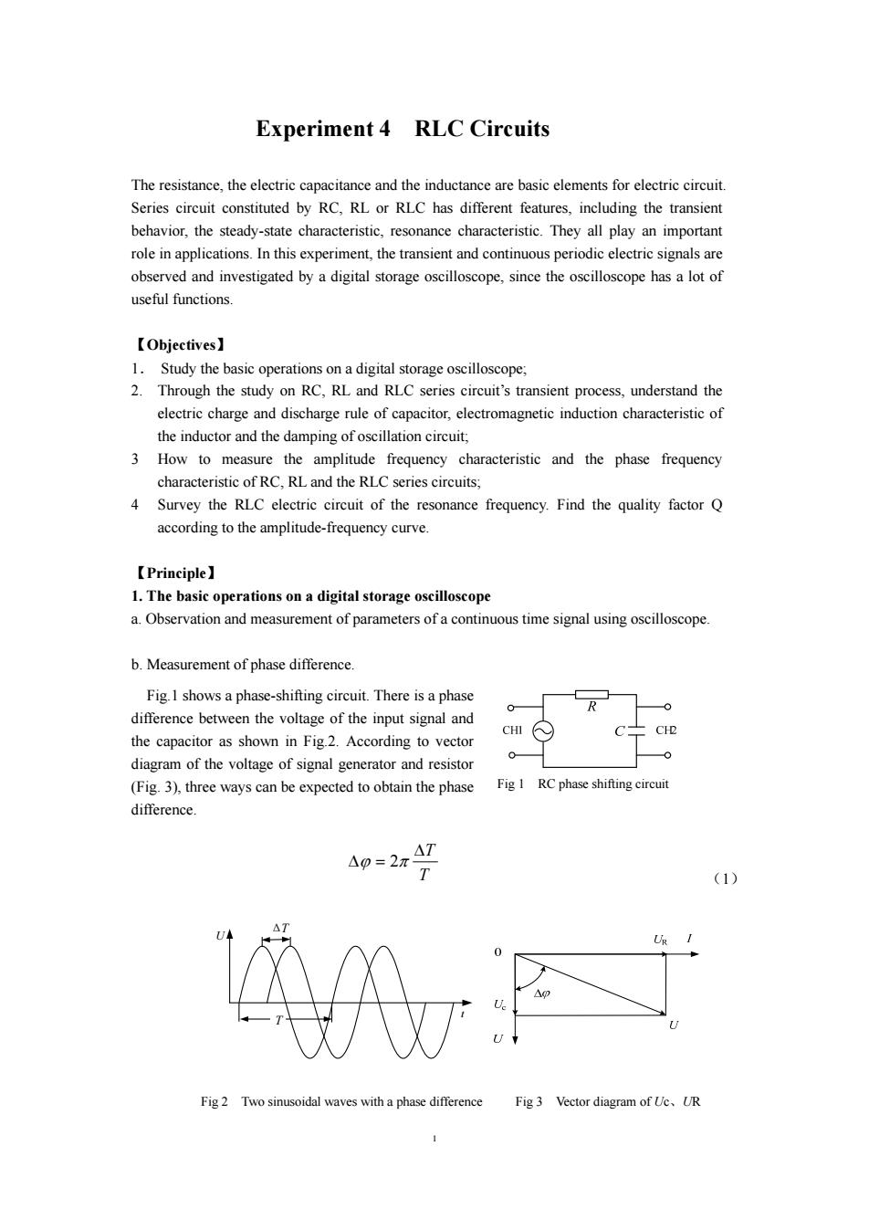
1 Experiment 4 RLC Circuits The resistance, the electric capacitance and the inductance are basic elements for electric circuit. Series circuit constituted by RC, RL or RLC has different features, including the transient behavior, the steady-state characteristic, resonance characteristic. They all play an important role in applications. In this experiment, the transient and continuous periodic electric signals are observed and investigated by a digital storage oscilloscope, since the oscilloscope has a lot of useful functions. 【Objectives】 1. Study the basic operations on a digital storage oscilloscope; 2. Through the study on RC, RL and RLC series circuit’s transient process, understand the electric charge and discharge rule of capacitor, electromagnetic induction characteristic of the inductor and the damping of oscillation circuit; 3 How to measure the amplitude frequency characteristic and the phase frequency characteristic of RC, RL and the RLC series circuits; 4 Survey the RLC electric circuit of the resonance frequency. Find the quality factor Q according to the amplitude-frequency curve. 【Principle】 1. The basic operations on a digital storage oscilloscope a. Observation and measurement of parameters of a continuous time signal using oscilloscope. b. Measurement of phase difference. Fig.1 shows a phase-shifting circuit. There is a phase difference between the voltage of the input signal and the capacitor as shown in Fig.2. According to vector diagram of the voltage of signal generator and resistor (Fig. 3), three ways can be expected to obtain the phase difference. T ΔT Δϕ = 2π (1) t U T ΔT Fig 2 Two sinusoidal waves with a phase difference Fig 3 Vector diagram of Uc、UR Fig 1 RC phase shifting circuit
c.Measurement of a transient signal (Optional) As is illustrated in Fig.4,a flashing lamp is a HID(High Intensity Discharge)light that is filled with high-pressured xenon gas,which would be swiftly ionized and form a voltaic arc when there is a high voltage between two electrodes,and meantime the resistance of which drops drastically so that a strong current occurs.An energy storing capacitor must be needed to maintain the discharging.The initial ionization is triggered by a high pressured impulse,and in the process of discharge,the energy stored in the capacitor is consumed swiftly and so is the voltage between the capacitor,so when the process are no longer able to be maintained,the flash ends.If the capacitance of the capacitor is small,this process is extremely short in the order of magnitude of microseconds. As for observing the flashing process,a proper photoelectric sensor should be chosen so that the response time will be as short as possible.Here we provide two types of photoelectric sensors. One is a silicon photoelectric diode of PIN type with a small area,which has a layer of intrinsic material that enables a lower capacity,a faster response and a better linear property when inversely biased.Another is Cds photosensitive resistor,whose response time is relatively long and which is not proper to be used for a quick measurement.Here the Cds is merely for a reference.The sampling resistance in the quick measurement also needs to be low in order to minimize the lost of the high-frequency part of the signal. In Fig.4,Ce is the energy-storing capacitor,R is the current sampling resistor in discharge process,R2 is the sampling resistor for the photoelectric current from photoelectric sensor D.Ce is in parallel with the flashing lamp.With this circuit,we can simultaneously measure the discharge current of capacitor Ce and the signal of flash. If the voltage between Ce is Ve and Va before and after discharging,then the total energy output of Ce is E.-c.- (2) We can also roughly estimate the power input Pr of the flashing lamp by taking the half-width of the photoelectric current at the time interval.However,Pr is much affected by the conversion efficiency of flash lamp. 90% 50% 10% Fig5 The transient signal of the two sampling resistors 2
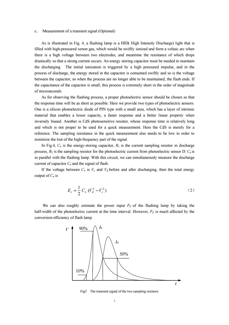
2 c. Measurement of a transient signal (Optional) As is illustrated in Fig. 4, a flashing lamp is a HID( High Intensity Discharge) light that is filled with high-pressured xenon gas, which would be swiftly ionized and form a voltaic arc when there is a high voltage between two electrodes, and meantime the resistance of which drops drastically so that a strong current occurs. An energy storing capacitor must be needed to maintain the discharging. The initial ionization is triggered by a high pressured impulse, and in the process of discharge, the energy stored in the capacitor is consumed swiftly and so is the voltage between the capacitor, so when the process are no longer able to be maintained, the flash ends. If the capacitance of the capacitor is small, this process is extremely short in the order of magnitude of microseconds. As for observing the flashing process, a proper photoelectric sensor should be chosen so that the response time will be as short as possible. Here we provide two types of photoelectric sensors. One is a silicon photoelectric diode of PIN type with a small area, which has a layer of intrinsic material that enables a lower capacity, a faster response and a better linear property when inversely biased. Another is CdS photosensitive resistor, whose response time is relatively long and which is not proper to be used for a quick measurement. Here the CdS is merely for a reference. The sampling resistance in the quick measurement also needs to be low in order to minimize the lost of the high-frequency part of the signal. In Fig.4, Ce is the energy-storing capacitor, R1 is the current sampling resistor in discharge process, R2 is the sampling resistor for the photoelectric current from photoelectric sensor D. Ce is in parallel with the flashing lamp. With this circuit, we can simultaneously measure the discharge current of capacitor Ce and the signal of flash. If the voltage between Ce is Vc and Vd before and after discharging, then the total energy output of Ce is ( ) 2 1 2 2 Ec = Ce Vd −Vc (2) We can also roughly estimate the power input PF of the flashing lamp by taking the half-width of the photoelectric current at the time interval. However, PF is much affected by the conversion efficiency of flash lamp. V t IR ID 10% 90% 50% Fig5 The transient signal of the two sampling resistors

Through the sampling resistance Ri,we can measure the peak voltage Vp of Ri and thus the peak power of the sampling resistance Ri is PR =Vp2 /R (3) The rising slope di/dt can be evaluated with reference to the change from the 10%to 90%of the peak value. 2.The transient process of RC.RL RLC circuits (1)series RC circuits. As shown in Fig.6,electric capacity charge and discharges during the transient process.The signal source supply square-wave signal.During the first half cycle,the voltage of source is +E.it charges the capacitor;the square-wave voltage turns to 0 in the second half cycle,the capacity discharges.The equation of charging process is Fig6 Series RC circuit RCUc+Ue=E dt (4) Initial condition:t=0 =>Uc=0, Uc=E(1-e RC) Ug =iR=Ee RC (5) From the equation of Uc,UR,Uc increases with time t by exponential law,while resistance voltage Ug decrease in the same way,as shown in Fig.7,therein displaying U-t Uc-t、UR-1 curves.. The equation of discharging process: Rcde+U。=0 UR dr (6) Initial condition:t=0,=>U=E thus we have Uc Ee R UR=R=-Ee旋 (8) From the equation of Uc.Ug,they both decay with time Fig 7 Charging and discharging by exponential law.RC=,which has the dimension of process of series RC circuit
3 Through the sampling resistance R1, we can measure the peak voltage VP of R1 and thus the peak power of the sampling resistance R1 is 1 2 1 PR = Vp / R (3) The rising slope di/dt can be evaluated with reference to the change from the 10% to 90% of the peak value. 2.The transient process of RC、RL、RLC circuits (1)series RC circuits. As shown in Fig. 6, electric capacity charge and discharges during the transient process. The signal source supply square-wave signal. During the first half cycle, the voltage of source is +E. it charges the capacitor; the square-wave voltage turns to 0 in the second half cycle, the capacity discharges. The equation of charging process is U E t U RC C C + = d d (4) Initial condition: t = 0 => UC = 0, RC t R RC t C U iR Ee U E e − − = = = (1− ) (5) From the equation of UC、UR , UC increases with time t by exponential law, while resistance voltage UR decrease in the same way, as shown in Fig.7, therein displaying U – t、 UC – t、UR – t curves. The equation of discharging process: 0 d d + C = C U t U RC (6) Initial condition: t = 0,=>UC = E thus we have RC t R RC t C U iR Ee U Ee − − = = − = (8) From the equation of UC、UR , they both decay with time by exponential law. RC =τ, which has the dimension of Fig 7 Charging and discharging process of series RC circuit Fig6 Series RC circuit

time,is called time constant.It is an important physical quantity to characterize the speed of transient process.Another characteristic number related with time constant r is so called half-value time Ti,which means half of time that Uc(t)decrease to its initial value or increase to a terminal value.It is also used to describe the speed of transient process.The relationship between Tin and r is: T12=ln2=0.693(ort=1.443T1n) (9) (2)series RL circuits The analysis is similar to RC circuits.Through which we can obtain the time constant r and half-value time Ti: ÷上,T2=0.693x=0.6931 (10) (3)series RLC circuit. Firstly,discuss the condition that a power supply is turned on suddenly,the equation of capacitor voltage Uc is LCU+RC Uc+Ve=E dt2 dt (11) Divide by LC on both sides,and let B=R/2L and 00= LC (12) Then the Eq.11 changes into: dU+260+U。=ogE dr2 dt (13) Eq.13 is a typical equation of damped oscillation.B is damping coefficient,@o is the natural frequency of the circuit.Together with the two initial condition of this process: dUc =0 =0:dr o (14) Therefore,the solution to Eq.13 depends on the ratio ofB and @o. 4
4 time, is called time constant. It is an important physical quantity to characterize the speed of transient process. Another characteristic number related with time constant τ is so called half-value time T1/2, which means half of time that UC(t)decrease to its initial value or increase to a terminal value. It is also used to describe the speed of transient process. The relationship between T1/2 and τ is: T1/2 =τln2 = 0.693(or τ = 1.443T1/2) (9) (2)series RL circuits The analysis is similar to RC circuits. Through which we can obtain the time constant τ and half-value time T1/2: R L T R L τ = , 1 / 2 = 0.693τ = 0.693 (10) (3)series RLC circuit. Firstly, discuss the condition that a power supply is turned on suddenly, the equation of capacitor voltage UC is U E t U RC t U LC C C C + + = d d d d 2 2 (11) Divide by LC on both sides,and let β = R 2L and LC 1 ω0 = (12) Then the Eq.11 changes into: U E t U t U C C C 2 0 2 2 0 2 d d 2 d d + β + ω =ω (13) Eq. 13 is a typical equation of damped oscillation. β is damping coefficient,ω0 is the natural frequency of the circuit.Together with the two initial condition of this process: 0 0 = C t= U ; 0 d d 0 = t= C t U (14) Therefore, the solution to Eq. 13 depends on the ratio of β and ω0.
The result is discussed under three different conditions as following: (1)underdamping wheniscalled underdamping,the solution is Uc=E-Ee-R cos+ (15) WhereEq.15 is called damping oscillation solution. (2)overdamping when0,it is called overdamping. The solution is Ue=E-号ele+水--7k 2r (16) Where,there is no oscillation in this case. (3)critical damping when0 it iscalled critical damping,the solution is U=E-E(1+Bte- (17) When the circuit achieves steady state,dropping the power supply suddenly(E-0),the changes periodic damping U square wave critical damping Fig8 Charge&discharge wave pattern of series RLC circuit
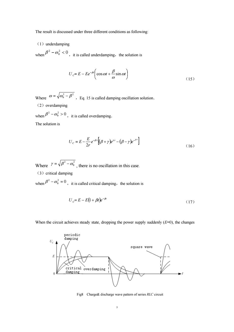
5 The result is discussed under three different conditions as following: (1)underdamping when 0 2 0 2 β −ω ,it is called overdamping. The solution is [( )( ) ]t t t C e e e r E U E 2 γ β γ β γ β γ − − = − + − − (16) Where 2 0 2 γ = β −ω , there is no oscillation in this case. (3)critical damping when 0 2 0 2 β −ω = ,it is called critical damping,the solution is ( ) t C U E E t e β β − = − 1+ (17) When the circuit achieves steady state, dropping the power supply suddenly (E=0), the changes Fig8 Charge& discharge wave pattern of series RLC circuit
on the circuit is similar to the charging process.The solutions of the equation also can be classified into three types. The discussion above is under the condition that the source supply step-function signal and the inherent resistance of source is zero.Practically,we can use a square wave source instead.The only restriction is the cyclic of it is much longer than the time constant of the circuit. Uc changes with t in the three different conditions as show in Fig8. 2.RC.RL steady-state circuit. When input simple sinusoidal alternating voltage U;into the series RC (or RL)circuit,the output voltage Uo of capacity or resistance Uo will change its amplitude and phase.To determine the Amplitude-frequency and phase-frequency relations,we only need to measure the voltage of various components under different input frequencies. p=g业=g必 UR R (18) 9=18=18( @CR (19) 3.RLC oscillation circuit. R -Uc C 0 Fig 9 Series RLC circuit (1)Fig.9 shows the series RLC circuit.Impedance and phase difference can be calculated through vector diagram,because the current in components is the same.Let current vector I be the horizontal benchmark.While the voltage of each component has a phase difference with current,which is 2,0--2 π PR=0 PL= 2 The effective voltage is Ug IZ IR,U IZ =IoL,Uc=IZc =1/@C (20) 6
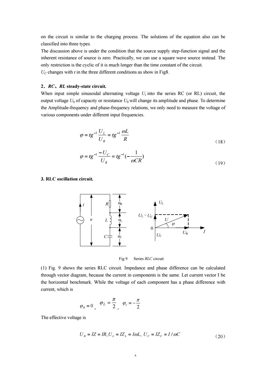
6 Fig 9 Series RLC circuit on the circuit is similar to the charging process. The solutions of the equation also can be classified into three types. The discussion above is under the condition that the source supply step-function signal and the inherent resistance of source is zero. Practically, we can use a square wave source instead. The only restriction is the cyclic of it is much longer than the time constant of the circuit. UC changes with t in the three different conditions as show in Fig8. 2.RC、RL steady-state circuit. When input simple sinusoidal alternating voltage Ui into the series RC (or RL) circuit, the output voltage U0 of capacity or resistance U0 will change its amplitude and phase. To determine the Amplitude-frequency and phase-frequency relations, we only need to measure the voltage of various components under different input frequencies. R L tg U U tg R L ω ϕ −1 −1 = = (18) ) 1 ( 1 1 CR tg U U tg R C ω ϕ = − − = − − (19) 3. RLC oscillation circuit. (1) Fig. 9 shows the series RLC circuit. Impedance and phase difference can be calculated through vector diagram, because the current in components is the same. Let current vector I be the horizontal benchmark. While the voltage of each component has a phase difference with current, which is ϕ R = 0 , 2 π ϕ L = , 2 π ϕc = − The effective voltage is U R = IZ = IR,U L = IZ L = IωL, UC = IZ C = I /ωC (20)
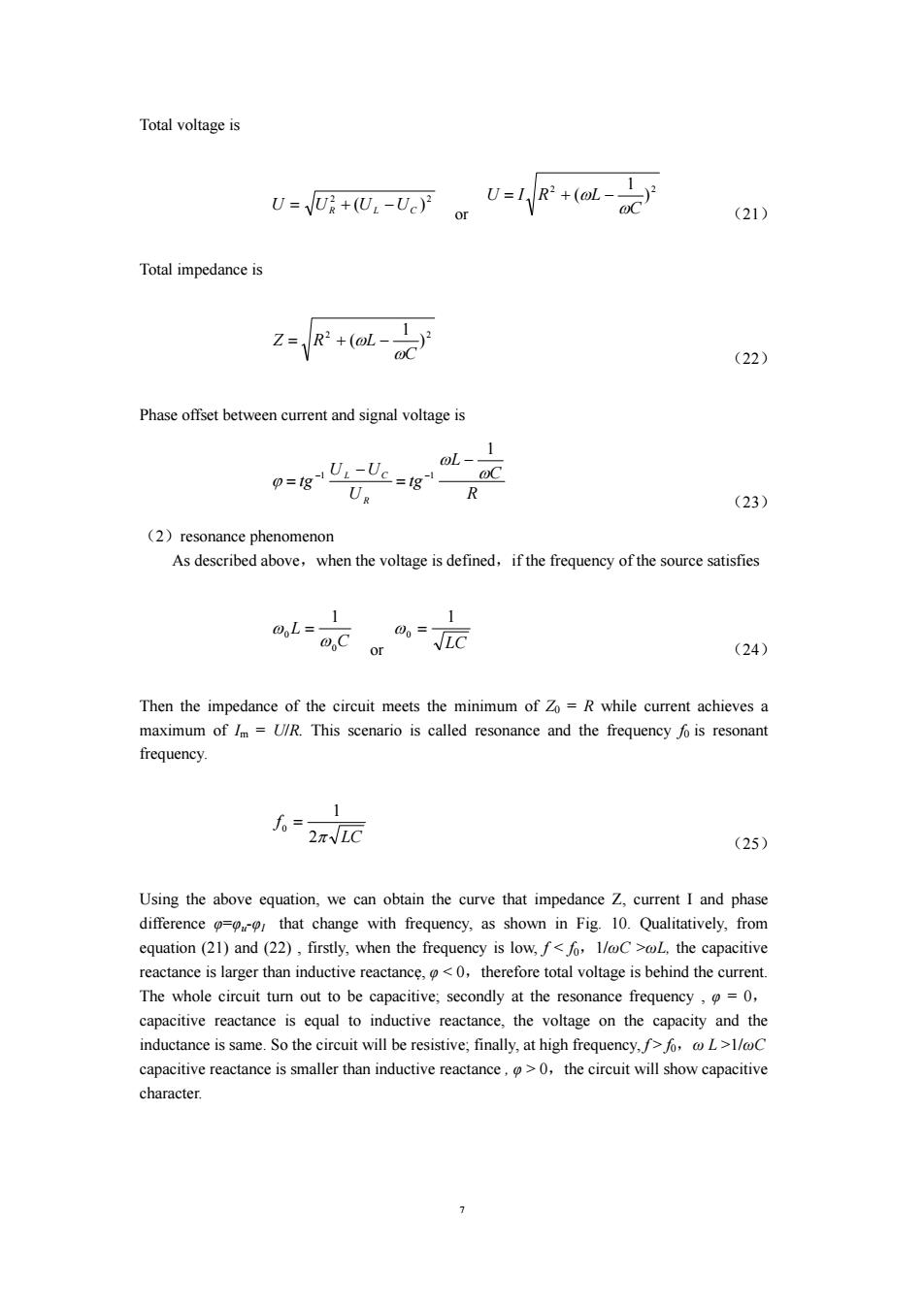
Total voltage is U--Vo)+(oL-oc (21) Total impedance is +a Z1 (22) Phase offset between current and signal voltage is 0L、1 UUc=OC UR R (23) (2)resonance phenomenon As described above,when the voltage is defined,if the frequency of the source satisfies 1 1 0L= C 00= or (24) Then the impedance of the circuit meets the minimum of Zo =R while current achieves a maximum of /m =U/R.This scenario is called resonance and the frequency fo is resonant frequency. 1 0=。 2πVLC (25) Using the above equation,we can obtain the curve that impedance Z,current I and phase difference that change with frequency,as shown in Fig.10.Qualitatively,from equation (21)and(22),firstly,when the frequency is low,foL,the capacitive reactance is larger than inductive reactance,fo,L>1/@C capacitive reactance is smaller than inductive reactance,0,the circuit will show capacitive character
7 Total voltage is 2 2 ( ) U = UR + UL −UC or 2 2 ) 1 ( C U I R L ω = + ω − (21) Total impedance is 2 2 ) 1 ( C Z R L ω = + ω − (22) Phase offset between current and signal voltage is R C L tg U U U tg R L C ω ω ϕ 1 1 1 − = − = − − (23) (2)resonance phenomenon As described above,when the voltage is defined,if the frequency of the source satisfies C L 0 0 1 ω ω = or LC 1 ω0 = (24) Then the impedance of the circuit meets the minimum of Z0 = R while current achieves a maximum of Im = U/R. This scenario is called resonance and the frequency f0 is resonant frequency. LC f 2π 1 0 = (25) Using the above equation, we can obtain the curve that impedance Z, current I and phase difference φ=φu-φI that change with frequency, as shown in Fig. 10. Qualitatively, from equation (21) and (22) , firstly, when the frequency is low, f ωL, the capacitive reactance is larger than inductive reactance, φ f0,ω L >1/ωC capacitive reactance is smaller than inductive reactance , φ > 0,the circuit will show capacitive character

π/2 -π/2 Jo ffof2 (a) (b) (c) Fig10 Resonant curve of the series resonant circuit and phase-frequency relation (3)quality factor of resonant circuit. (I)definition of O and the voltage allocation. From Im=U/R,we can obtain the voltage of resistor,capacitor and inductor is UR=IR=U U U1=1nZ,=元0L R (26) U,1 Uc-1aZe=RoC =UL While resonance occurs,the ratio of inductor voltage UL(or voltage on capacitor U)to the total voltage is called quality factor,denoted by 0=4-0L0= U R or U @RC (27) When the total voltage is fixed,higher the is,larger UL and Uc are.O is a physical quantity to characterize the quality of a resonant circuit. (II)the frequency selectivity of resonant circuit. The most important application of resonant circuits in wireless technology is signal selection.In order to illustrate the quality of frequency selectivity,usually the bandwidth is defined as the distance betweenon both side of the resonant peak.sshown in Fig.11 △f=方2-f (28) =U)-方 (29) It can be proved that the bandwidth Af is inversely proportional to Q,thus
8 (3)quality factor of resonant circuit. (I)definition of Q and the voltage allocation. From Im = U/R,we can obtain the voltage of resistor, capacitor and inductor is UR = I m R = U L R U UL = I m ZL = ω0 (26) C m C U L R C U U = I Z = ⋅ = 0 1 ω While resonance occurs, the ratio of inductor voltage UL (or voltage on capacitor Uc) to the total voltage is called quality factor, denoted by Q R L U U Q L ω0 = = or U RC U Q ω0 C 1 = = (27) When the total voltage is fixed, higher the Q is , larger UL and UC are. Q is a physical quantity to characterize the quality of a resonant circuit. (II)the frequency selectivity of resonant circuit. The most important application of resonant circuits in wireless technology is signal selection. In order to illustrate the quality of frequency selectivity, usually the bandwidth is defined as the distance between ( ) m I = 1 2 I on both side of the resonant peak. As shown in Fig. 11 2 1 Δf = f − f (28) () ( ) 2 1 2 mI I f = I f = (29) It can be proved that the bandwidth Δf is inversely proportional to Q , thus O f R Z f 0 f 0 f 1 f 2 O I I m I m 2 f f 0 O f (a) (b) (c) Fig10 Resonant curve of the series resonant circuit and phase-frequency relation

4r=6 (30) The bigger is,the smaller Af will be.Thus the resonant peak will be sharper.Therefore the frequency selectivity will be better is a bigger Q is chosen. 【Equipment】 Digital multimeter,digital capacitance table,power function signal generator,digital storage oscilloscope,transistors millivoltmeter experiment wiring boards,resistance,capacitance, inductance,flash generator;and photo sensor and so on. 【Experiment】 1.Observe alternative current waves produced by a signal generator.The signals include a sinusoidal wave,square wave,triangular waves,impulse wave and TTL (transistor-transistor logic)wave.Roughly draw the waves.Record the peak-to peak value,period or frequency. 2.Connect the phase-shifting circuit as shown in Fig.1.Use the "cursor"of the oscillator to measure the phase difference between the voltage of the input signal and the capacitor,Find 3 frequencies which make the differences close to 0 degree,at 45 degree and close to 90 degree,respectively.Draw the vector diagram as is illustrated by Fig.3. 3.(Optional)Connect the circuit as in Fig.4.Double-check the circuit and then connect the power.When the indicator of the flash generator is on,push the trigger button.After that there should be a flash generated,then,adjust the trigger mode of the oscilloscope so that it is in the single triggered mode.Properly adjust the trigger voltage and the channel sensitivity, and two sampled waves will be on the screen as in Fig.5.To properly measure the residual voltage,disconnect the power switch K,and try not to touch the electrodes of the capacitor when changing the energy storing capacitor.When removing the capacitors,make sure that the capacitors are discharged.In order to make the silicon photoelectric diode D to always be biased inversely,the position of D and the flashing lamp should be adjusted so that the lowest voltage on D is about 3V. 4.Choose various RC or RL to build up series circuits.Measure and describe the wave pattern of capacity or inductance when time constant is larger or smaller than the cycle of the square wave.Calculate the time constant and compare it with the theoretical value. 5.Choose various RLC to build up series circuits.Measure and describe the capacitor voltage during underdamping,critical damping and overdamping process.Calculate the time constant and compare it to the theoretical value.Notice that the cycle of square wave should be much longer than the time constant. 6.Input simple sinusoidal alternating voltage U;to the RC and RL series circuit.Plot the amplitude-frequency and phase frequency curve under the same time axis.The amplitude should be represented in relative change. 7.Input simple sinusoidal alternating voltage U;to the series RLC circuit.Measure the component voltage or various components changing with the frequency of Ui.Plot the amplitude-frequency and phase frequency curve.The requirement is the same to item 6. Determine the resonant frequency,calculate the quality factor,choose 20 different frequencies respectively.Take another capacitor to make a comparison
9 Q f f 0 Δ = (30) The bigger Q is, the smaller Δf will be. Thus the resonant peak will be sharper. Therefore the frequency selectivity will be better is a bigger Q is chosen. 【Equipment】 Digital multimeter, digital capacitance table, power function signal generator, digital storage oscilloscope, transistors millivoltmeter experiment wiring boards, resistance, capacitance, inductance, flash generator; and photo sensor and so on. 【Experiment】 1. Observe alternative current waves produced by a signal generator. The signals include a sinusoidal wave, square wave, triangular waves, impulse wave and TTL (transistor-transistor logic) wave. Roughly draw the waves. Record the peak-to peak value, period or frequency. 2. Connect the phase-shifting circuit as shown in Fig.1. Use the “cursor” of the oscillator to measure the phase difference between the voltage of the input signal and the capacitor, Find 3 frequencies which make the differences close to 0 degree, at 45 degree and close to 90 degree, respectively. Draw the vector diagram as is illustrated by Fig. 3. 3. (Optional) Connect the circuit as in Fig.4. Double-check the circuit and then connect the power. When the indicator of the flash generator is on, push the trigger button. After that there should be a flash generated, then, adjust the trigger mode of the oscilloscope so that it is in the single triggered mode. Properly adjust the trigger voltage and the channel sensitivity, and two sampled waves will be on the screen as in Fig. 5 . To properly measure the residual voltage, disconnect the power switch K, and try not to touch the electrodes of the capacitor when changing the energy storing capacitor. When removing the capacitors, make sure that the capacitors are discharged. In order to make the silicon photoelectric diode D to always be biased inversely, the position of D and the flashing lamp should be adjusted so that the lowest voltage on D is about 3V. 4. Choose various RC or RL to build up series circuits. Measure and describe the wave pattern of capacity or inductance when time constant is larger or smaller than the cycle of the square wave. Calculate the time constant and compare it with the theoretical value. 5. Choose various RLC to build up series circuits. Measure and describe the capacitor voltage during underdamping, critical damping and overdamping process.Calculate the time constant and compare it to the theoretical value. Notice that the cycle of square wave should be much longer than the time constant. 6. Input simple sinusoidal alternating voltage Ui to the RC and RL series circuit. Plot the amplitude-frequency and phase frequency curve under the same time axis. The amplitude should be represented in relative change. 7. Input simple sinusoidal alternating voltage Ui to the series RLC circuit. Measure the component voltage or various components changing with the frequency of Ui. Plot the amplitude-frequency and phase frequency curve. The requirement is the same to item 6. Determine the resonant frequency, calculate the quality factor, choose 20 different frequencies respectively. Take another capacitor to make a comparison
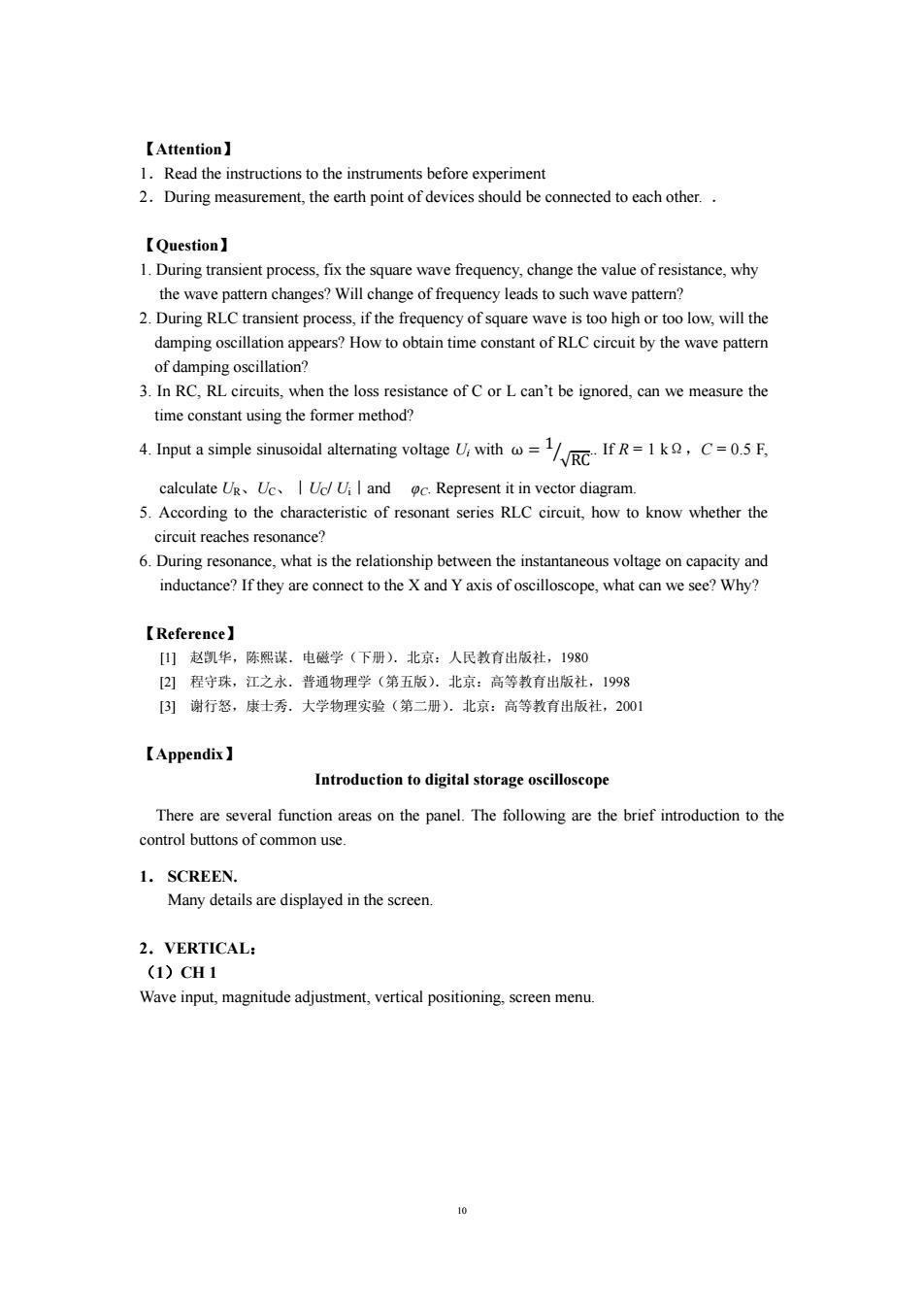
【Attention】 1.Read the instructions to the instruments before experiment 2.During measurement,the earth point of devices should be connected to each other.. 【Question】 1.During transient process,fix the square wave frequency,change the value of resistance,why the wave pattern changes?Will change of frequency leads to such wave pattern? 2.During RLC transient process,if the frequency of square wave is too high or too low,will the damping oscillation appears?How to obtain time constant of RLC circuit by the wave pattern of damping oscillation? 3.In RC,RL circuits,when the loss resistance of C or L can't be ignored,can we measure the time constant using the former method? 4.Input a simple sinusoidal altemating votage U,withIfRIkCF. calculate UR Uc.IU/U:I and c.Represent it in vector diagram. 5.According to the characteristic of resonant series RLC circuit,how to know whether the circuit reaches resonance? 6.During resonance,what is the relationship between the instantaneous voltage on capacity and inductance?If they are connect to the X and Y axis of oscilloscope,what can we see?Why? 【Reference】 []赵凯华,陈熙谋.电磁学(下册).北京:人民教育出版社,1980 [2]程守珠,江之永.普通物理学(第五版).北京:高等教育出版社,1998 [3)谢行怒,康士秀.大学物理实验(第二册).北京:高等教育出版社,2001 【Appendix】 Introduction to digital storage oscilloscope There are several function areas on the panel.The following are the brief introduction to the control buttons of common use. 1.SCREEN. Many details are displayed in the screen. 2.VERTICAL: (1)CH1 Wave input,magnitude adjustment,vertical positioning,screen menu
10 【Attention】 1.Read the instructions to the instruments before experiment 2.During measurement, the earth point of devices should be connected to each other. . 【Question】 1. During transient process, fix the square wave frequency, change the value of resistance, why the wave pattern changes? Will change of frequency leads to such wave pattern? 2. During RLC transient process, if the frequency of square wave is too high or too low, will the damping oscillation appears? How to obtain time constant of RLC circuit by the wave pattern of damping oscillation? 3. In RC, RL circuits, when the loss resistance of C or L can’t be ignored, can we measure the time constant using the former method? 4. Input a simple sinusoidal alternating voltage Ui with ω ൌ 1 √RC ൗ .. If R = 1 kΩ,C = 0.5 F, calculate UR、UC、|UC/ Ui|and φC. Represent it in vector diagram. 5. According to the characteristic of resonant series RLC circuit, how to know whether the circuit reaches resonance? 6. During resonance, what is the relationship between the instantaneous voltage on capacity and inductance? If they are connect to the X and Y axis of oscilloscope, what can we see? Why? 【Reference】 [1] 赵凯华,陈熙谋.电磁学(下册).北京:人民教育出版社,1980 [2] 程守珠,江之永.普通物理学(第五版).北京:高等教育出版社,1998 [3] 谢行怒,康士秀.大学物理实验(第二册).北京:高等教育出版社,2001 【Appendix】 Introduction to digital storage oscilloscope There are several function areas on the panel. The following are the brief introduction to the control buttons of common use. 1. SCREEN. Many details are displayed in the screen. 2.VERTICAL: (1)CH 1 Wave input, magnitude adjustment, vertical positioning, screen menu