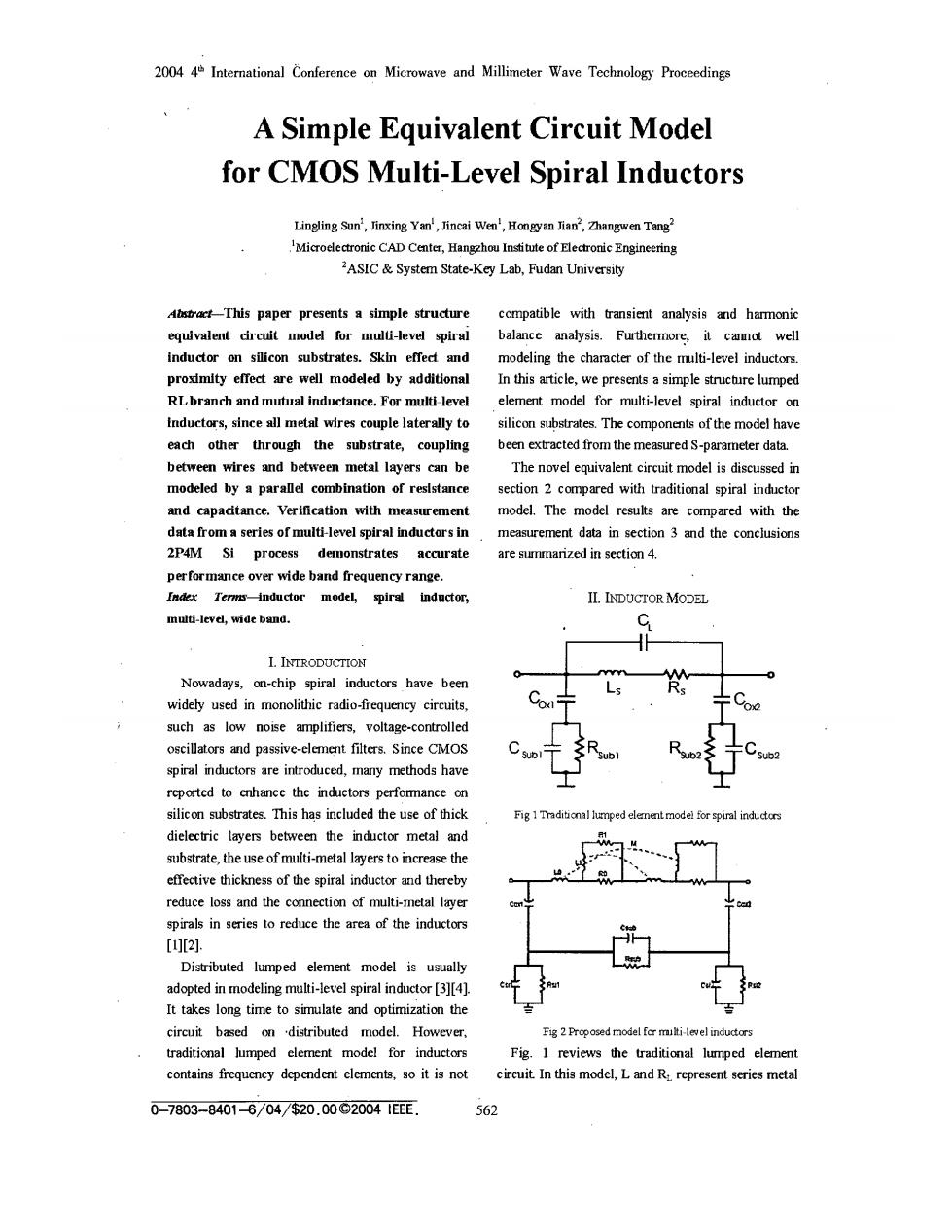
2004 4 International Conference on Microwave and Millimeter Wave Technology Proceedings A Simple Equivalent Circuit Model for CMOS Multi-Level Spiral Inductors Lingling Sun',Jinxing Yan',Jincai Wen',Hongyan Jian?,Zhangwen Tang? IMicroelectronic CAD Center,Hangzhou Institute of Electronic Engineering 2ASIC System State-Key Lab,Fudan University Atstract-This paper presents a simple structure compatible with transient analysis and harmonic equivalent circuit model for multi-level spiral balance analysis.Furthermore,it cannot well inductor on silicon substrates.Skin effect and modeling the character of the rrulti-level inductors. proximity effect are well modeled by additional In this article,we presents a simple structure lumped RL branch and mutual inductance.For multi-level element model for multi-level spiral inductor on Inductors,since all metal wires couple laterally to silicon substrates.The components of the model have each other through the substrate,coupling been extracted from the measured S-parameter data. between wires and between metal layers can be The novel equivalent circuit model is discussed in modeled by a parallel combination of reslstance section 2 compared with traditional spiral inductor and capacitance.Verification with measurement model.The model results are compared with the data from a series of multi-level spiral inductors in measurement data in section 3 and the conclusions 2P4M Si process demonstrates accurate are summarized in section 4. performance over wide band frequency range. Iadex Terms-inductor model,spiral inductor, II.INDUCTOR MODEL multi-level,wide band. I.INTRODUCTION Y Nowadays,on-chip spiral inductors have been Ls Rs widely used in monolithic radio-frequency circuits, C0 such as low noise amplifiers,voltage-controlled oscillators and passive-element filters.Since CMOS C R R Subl 2 Sub2 spiral inductors are introduced,many methods have reported to enhance the inductors performance on silicon substrates.This has included the use of thick Fig 1 Traditional lumped elenent model for spiral inductors dielectric layers between the inductor metal and substrate,the use of multi-metal layers to increase the effective thickness of the spiral inductor and thereby reduce loss and the connection of multi-metal layer ced spirals in series to reduce the area of the inductors [1][2]. Distributed lumped element model is usually adopted in modeling multi-level spiral inductor [3][4]. P2 It takes long time to simulate and optimization the circuit based on distributed model.However, Fig 2 Proposed model for mmilti-level inductors traditional lumped element model for inductors Fig.1 reviews the traditional lumped element contains frequency dependent elements,so it is not circuit.In this model,L and R represent series metal 0-7803-8401-6/04/$20.00©20041EEE. 562

inductance and resistance,C modeling fringing and Dielectric isolation capacitance are modeled by Cox. feed-through capacitance,Cox modeling dielectric and substrate loss Rsus and CsuB are also modeled. isolation capacitance.Substrate loss RsuB and CsuB Feed-through capacitance modeling the parasitic are also modeled.Extracted Ls and Rs are capacitive coupling between input and output ports of frequency-dependent,model based on these the spiral inductor is neglected,due to existent parameters is not compatible with transient aalysis. capacitive coupling through Coxi,CsuB and Cox. A common compromise is to extract L and R at a specific frequency and use these fixed values for further circuit simulation and optimization.While in wide band MMIC design,this approach will introduce significant error.Furthermore,for multi-level inductors,mutual inductance between layers and mutual inductance between metal wires cannot neglect.Traditional model,which not model Fig 3 four-turn four-metal-layer inductor with pattemed ground these effects,is inappropriate for multi-level shields inductors. In this paper,we propose a new equivalent circuit IND 1 IND 2 4 model for Multi-level spiral inductors (Fig 2).The via problems mentioned above are well solved. As we all know,the DC current is uniformly distributed inside a single metal wire,it can be modeled as Lo and Ro in series.At high frequencies. Silicon Substrate the current flow is limited to the outer surface of the metal wire,in order to represent the skin effect, additional RL branches can be added in parallel to Ro Fig 4 Cross-sectional view of the muiti-level inductors [1. Due to the close proximity between wires in a IⅡ.MODEL VERIFICATION spiral inductor,the current in each segment can In order to verify proposed model in this article, induce eddy currents in other segments and cause the two multi-level inductors were fabricated using resistance to increase,causing deterioration of Q.In standard 0.35 um CMOS process,with four metal [6],stacked wires have large mutual coupling levels on silicon substrate of 882-cm resistivity. coefficient K and as a result,the mutually induced Pattered ground shields (PGSs)were used to eddy current is more significant compared to the improve the performance of inductors by decoupling adjacent wires in the same layer.So mutual the inductor from the substrate [8],seen in fig 3. inductance M should be modeled in multi-level Spiral inductor IND 1 are formed using top metal inductors. layer (M4)and third metal layer (M3),while IND 2 For multi-level inductors,since all metal wires are formed using all four metal layers supplied in the couple laterally through the substrate,coupling process.Shunt structures between layers are realized between wires and coupling between metal layers can through vias.Fig 4 shows the sketch map of the both be represented by a parallel combination of Rsus and multi-level inductors.The structures of the inductors CsuB.The shunt RC structure has been addressed in are summarized in Table I.Both inductors were the distributed model [7],while our model can save measured by Agilent 8719ES from 50MHz to 8GHz. much time due to its simple structure. Fig 2 shows the ultimate equivalent circuit model proposed for multi-level on-chip inductors. 563

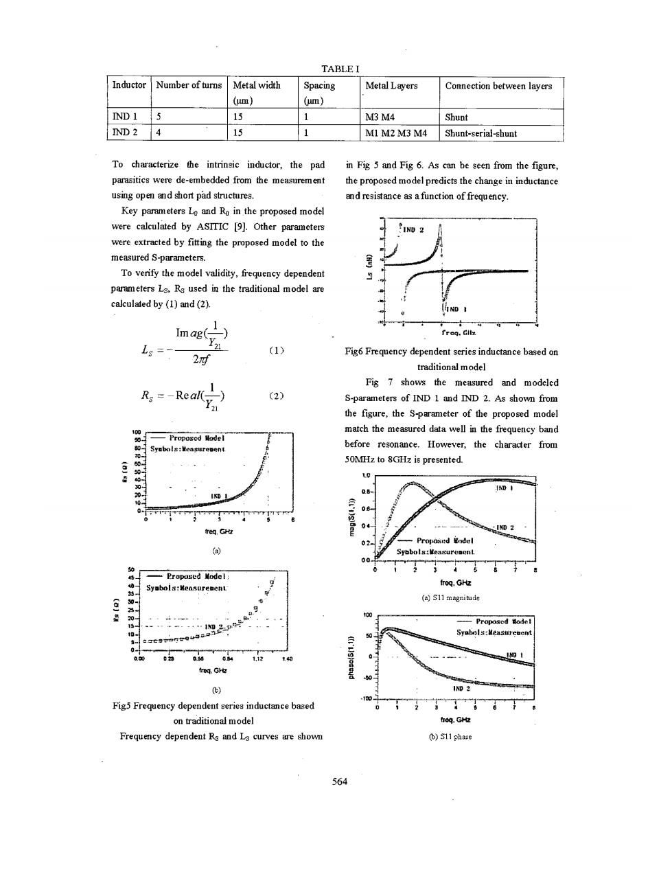
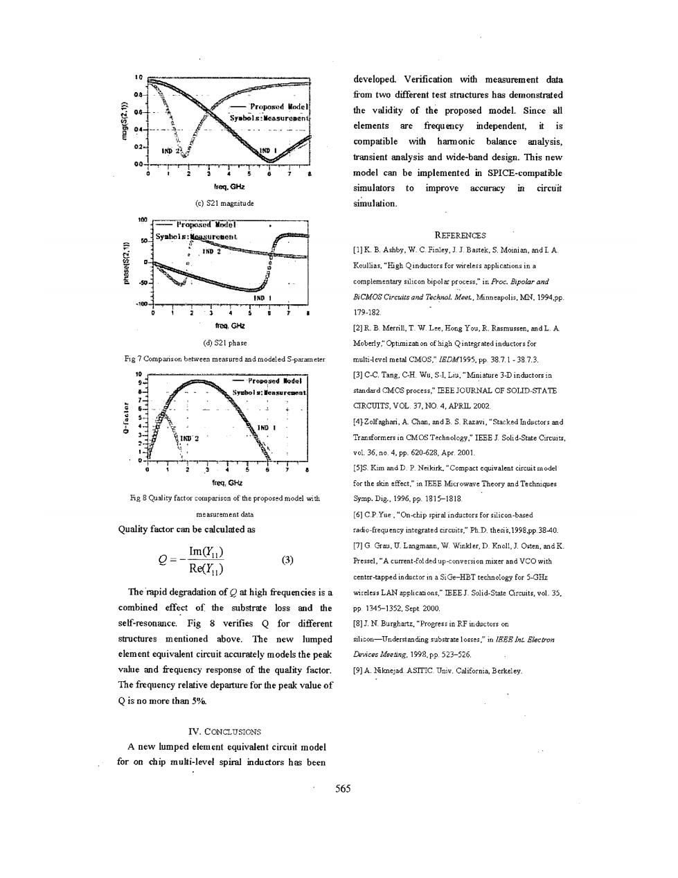
TABLE I Inductor Number of turns Metal width Spacing Metal Layers Connection between layers (um) (um IND1 5 1 M3 M4 Shunt IND 2 4 15 1 MI M2 M3 M4 Shunt-serial-shunt To characterize the intrinsic inductor,the pad in Fig 5 and Fig 6.As can be seen from the figure, parasitics were de-embedded from the measurement the proposed model predicts the change in inductance using open and short pad structures. and resistance as a function of frequency. Key parameters Lo and Ro in the proposed model were calculated by ASITIC [9].Other parameters IND 2 were extracted by fitting the proposed model to the measured S-parameters. To verify the model validity,frequency dependent parameters Ls,Rs used in the traditional model are calculated by (1)and (2). freg.Gllz Ls (1) 2时 Fig6 Frequency dependent series inductance based on traditional model 1 Fig 7 shows the measured and modeled Rs =-Real( (2) S-parameters of IND 1 and IND 2.As shown from the figure,the S-parameter of the proposed model match the measured data well in the frequency band 905 Proposed Hodel Syebols:能ea#trenent before resonance. However,the character from 50MHz to 8GHz is presented. 8 1.0 08- 0- ('))w 04 02 Proposed Eodel () Syobols:Weasurenent 00 5的 格 -Prapased Model: frog.GHz Syabols:Measurement (a)S11 magnitude 6 30- Proposed Hodel 0 ((I'L)Sjostyd 0 IND I 啊Ge 0 ) IND 2 Fig5 Frequency dependent series inductance based on traditional model trog.GHz Frequency dependent Rs and Ls curves are shown (b)S11 phase 564

40 developed.Verification with measurement data from two different test structures has demonstrated (('Z)s)6ow Proposod Model the validity of the proposed model.Since all Syobols:Measurepent elements are frequency independent,it is compatible with harmonic balance analysis, transient analysis and wide-band design.This new 00 model can be implemented in SPICE-compatible heg.GHz simulators to improve accuracy in circuit (c)S21 magnitude simulation. 00 —Proposed6d6T Syahols: REFERENCES [1]K.B.Ashby,W.C.Finley.J.J.Bastek,5.Moinian,and I.A Koullias,"High Qinductors for wireless applications in a complementary silicon bipolar process,"in Proc.Bipolar and BiCMOS Circuits and Technol.Meet,Minneapolis,Mhl.1994.pp 179-182 freg.GHz [2]R.B.Merrill,T.W.Lee,Hong You,R.Rasmussen,andL.A (d)$21 phase Moberly,"Optimiranon of high Qintegrated inductors for Fig 7 Comparison between measured and modeled S-parameter multi-evel metal CMOS,"IDM1995.pp.38.7.1-38.7.3. p [3]C-C.Tang,C-H.Wu.S-I.Liu,"Miniature 3-D inductors in 一Proposed lodel Syebol s: standard CMCS process,"IEEE JOURNAL OF SOLID-STATE 7 CIRCUITS,VOL.37,NO.4,APRIL 2002. 5 4 [4]Zolfaghari,A.Chan,and B.S.Razavi."Stacked Inductor:and 3 Transformers in CMOS Technology,"IEEE J.Solid-State Circuits, vol.36,n0.4,Pp.620-628.Apt.2001 3 [5]S.Kim and D.P.Neikirk."Compact equivalent circuit model freq,GHz for the skin effect,"in TEEE Microwave Theory and Techniques Fig B Quality factor comparisen of the proposed model with Symp.Dig,1996.pp.1815-1818 measurement data [6]CP.Yue"On-chip piral inductors for siicon-based Quality factor can be calculated as radio-frequency integrated circuits."Ph.D.thesis.1998.pp.38-40. [7]G.Grau.U.Langmann,W.Winkler,D.Knoll,J.Osten,and K. 0= Im(Y) Re(Y) (3) Pressel,"A current-fol ded up-conversion mixer and VCO with center-tappedindctor inaSiGe-HBTtechnology for 5-GHz The rapid degradation of at high frequencies is a wireless LAN applications,"IEEE J.Solid-State Circuits,vol.35. combined effect of the substrate loss and the Pp1345-1352.5ept2000 self-resonance.Fig 8 verifies Q for different [8]J.N.Burghartz."Progress in RF inductors on structures mentioned above.The new lumped silicon-Understanding substr ate losses,"in /EBB int Blectron element equivalent circuit accurately models the peak Devices Meeting.1998.pp.523-526. value and frequency response of the quality factor. [9]A.Niknejad ASITIC.Univ.California,Berkeley The frequency relative departure for the peak value of Q is no more than 5%. IV.CONCLUSIONS A new lumped element equivalent circuit model for on chip multi-level spiral inductors has been 565