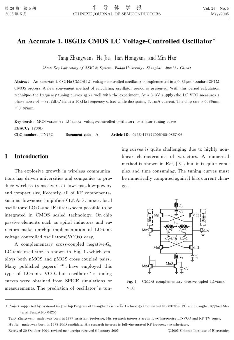
第26卷第5期 半导体学报 Vol.26 No.5 2005年5月 CHINESE JOURNAL OF SEMICONDUCTORS May,2005 An Accurate 1.08GHz CMOS LC Voltage-Controlled Oscillator* Tang Zhangwen,He Jie,Jian Hongyan,and Min Hao (State Key Laboratory of ASIC 8.System.Fudan University,Shanghai 200433,China) Abstract:An accurate 1.08GHz CMOS LC voltage-controlled oscillator is implemented in a 0.35um standard 2P4M CMOS process.A new convenient method of calculating oscillator period is presented.With this period calculation technique,the frequency tuning curves agree well with the experiment.At a 3.3V supply,the LC-VCO measures a phase noise of -82.2dBc/Hz at a 10kHz frequency offset while dissipating 3.ImA current.The chip size is 0.86mm X0.82mm. Key words:MOS varactor:LC tank;voltage-controlled oscillator;oscillator tuning curve EEACC:1230B CLC number:TN752 Document code:A Article1D:0253-4177(2005)05-0867-06 ing curves is quite challenging due to highly non- 1 Introduction linear characteristics of varactors.A numerical method is shown in Ref.[3],but it is quite com- The explosive growth in wireless communica- plex and time-consuming.The tuning curves must tions has driven universities and companies to pro- be numerically computed again if bias current chan- duce wireless transceivers at low-cost,low-power, ges. and compact size.Recently,all of RF components, such as low-noise amplifiers (LNAs),mixer,local oscillators(LOs),and IF filters,seem possible to be L 口 integrated in CMOS scaled technology.On-chip Mp LMp2| passive elements such as spiral inductors and va- V ractors make on-chip implementation of LC-tank Mn5 0-0 HMn6 voltage-controlled oscillators(VCOs)easy. A complementary cross-coupled negative-Gm MnL Mn2 LC-tank oscillator is shown in Fig.1,which em- ploys both nMOS and pMOS cross-coupled pairs. Mn3 Many published papers[i-3],have employed this Mn4H type of LC-tank VCO,but oscillator's tuning 1工 curves were obtained from SPICE simulations or Fig.1 CMOS complementary cross-coupled LC-tank measurements.The prediction of oscillator's tun- VCO Project supported by System-Design-Chip Program of Shanghai Science &Technology Committee(No.037062019)and Shanghai Applied Ma- terial Funds(No.0425) Tang Zhangwen male,was born in 1977,assistant professor.His research interests are in low-phase-noise LC-VCO and RF TV tuner. He Jie male,was born in 1978,PhD candidate.His research interest is fully-integrated RF frequency synthesizers. Received 30 October 2004.revised manuscript received 6 January 2005 ©2005 Chinese Institute of Electronics
第XW卷 第C期 X[[C年C月 半 导 体 学 报 NOLFV,V?R_6FE7R@,VQLNRF4_N’R6, \=%cXW F=cC Q*&!X[[C #K1=>$H28(..=12$#+&,&82$-/4$8"3)/N=C:.EQ0[/6%14/789>;R=P/8F>?899=K%@MH99;>8?# ’*)3;J6)J:!;,’(*,’) X[[aDD!!,)(’# "J@>?;M>$E)*HH(1*2$YZ[B0OUNQR,7NG=%2*3$/H=)21=%%$#=8H"%%*2=1"8"-.%$-$)2$#")*[ZDC$-82*)#*1#XKaQ NQR,.1=H$88cE)$]H=)G$)"$)2-$2M8K=$E "?>HM9=’$$[XCD/aYPP"X[[C#[C/[BWP/[W C ’F>?8KIM>H8F ’<$$T.%=8"G$31=]2<")]"1$%$88H=--()"H*/ 2"=)8<*8#1"G$)()"G$18"2"$8*)#H=-.*)"$82=.1=/ #(H$]"1$%$8821*)8H$"G$18*2%=]/H=82!%=]/.=]$1! *)#H=-.*H28"U$c6$H$)2%&!*%%=A6@H=-.=)$)28! 8(H<*8%=]/)="8$*-.%"A"$18"7FE8#!-"T$1!%=H*% =8H"%%*2=18"7R8#!*)#L@A"%2$18!8$$-.=88"+%$2=+$ ")2$31*2$#") NQR, 8H*%$# 2$H<)=%=3&cR)/H<". .*88"G$$%$-$)288(H<*88."1*%")#(H2=18*)#G*/ 1*H2=18 -*I$=)/H<"."-.%$-$)2*2"=)=A7N/2*)I G=%2*3$/H=)21=%%$#=8H"%%*2=18"\NR8#$*8&c E H=-.%$-$)2*1& H1=88/H=(.%$# )$3*2"G$/@- 7N/2*)I=8H"%%*2=1"88<=])")@"3cY!]<"H<$-/ .%=&8+=2<)QR,*)#.QR,H1=88/H=(.%$#.*"18c Q*)& .(+%"8<$# .*.$18’Y’D(!<*G$ $-.%=&$#2<"8 2&.$=A 7N/2*)I \NR!+(2 =8H"%%*2=1)82()")3 H(1G$8]$1$=+2*")$#A1=- ,KLNV8"-(%*2"=)8=1 -$*8(1$-$)28c’<$.1$#"H2"=)=A=8H"%%*2=1)82()/ ")3H(1G$8"8J("2$H<*%%$)3")3#($2=<"3<%&)=)/ %")$*1 H<*1*H2$1"82"H8 =A G*1*H2=18cE )(-$1"H*% -$2<=#"88<=])")6$Ac’D(!+(2"2"8J("2$H=-/ .%$T*)#2"-$/H=)8(-")3c’<$2()")3H(1G$8-(82 +$)(-$1"H*%%&H=-.(2$#*3*")"A+"*8H(11$)2H<*)/ 3$8c @"3cY NQR,H=-.%$-$)2*1&H1=88/H=(.%$#7N/2*)I \NR
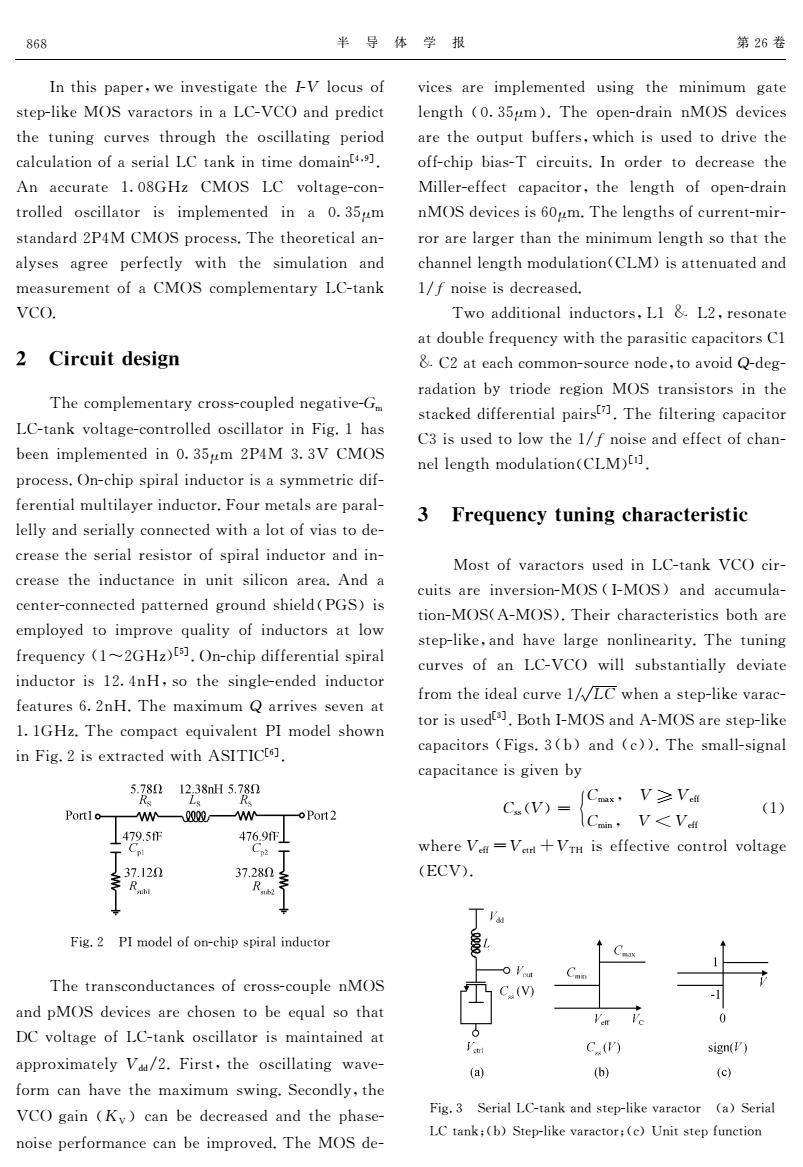
868 半导体学报 第26卷 In this paper,we investigate the IV locus of vices are implemented using the minimum gate step-like MOS varactors in a LC-VCO and predict length (0.35um).The open-drain nMOS devices the tuning curves through the oscillating period are the output buffers,which is used to drive the calculation of a serial LC tank in time domaint4.. off-chip bias-T circuits.In order to decrease the An accurate 1.08GHz CMOS LC voltage-con- Miller-effect capacitor,the length of open-drain trolled oscillator is implemented in a 0.35um nMOS devices is 60um.The lengths of current-mir- standard 2P4M CMOS process.The theoretical an- ror are larger than the minimum length so that the alyses agree perfectly with the simulation and channel length modulation(CLM)is attenuated and measurement of a CMOS complementary LC-tank 1/f noise is decreased. VCO. Two additional inductors,Ll &L2,resonate at double frequency with the parasitic capacitors Cl 2 Circuit design &C2 at each common-source node,to avoid Q-deg- radation by triode region MOS transistors in the The complementary cross-coupled negative-Gm stacked differential pairs.The filtering capacitor LC-tank voltage-controlled oscillator in Fig.1 has C3 is used to low the 1/f noise and effect of chan- been implemented in 0.35um 2P4M 3.3V CMOS nel length modulation(CLM). process.On-chip spiral inductor is a symmetric dif- ferential multilayer inductor.Four metals are paral- 3 Frequency tuning characteristic lelly and serially connected with a lot of vias to de- crease the serial resistor of spiral inductor and in- Most of varactors used in LC-tank VCO cir- crease the inductance in unit silicon area.And a cuits are inversion-MOS(I-MOS)and accumula- center-connected patterned ground shield(PGS)is tion-MOS(A-MOS).Their characteristics both are employed to improve quality of inductors at low step-like,and have large nonlinearity.The tuning frequency (1~GHz).On-chip differential spiral curves of an LC-VCO will substantially deviate inductor is 12.4nH,so the single-ended inductor from the ideal curve 1/VLC when a step-like varac- features 6.2nH.The maximum Q arrives seven at tor is usedt.Both I-MOS and A-MOS are step-like 1.1GHz.The compact equivalent PI model shown in Fig.2 is extracted with ASITIC]. capacitors (Figs.3(b)and (c)).The small-signal capacitance is given by 5.78212.38nH5.78 Rs Cmax,V≥V Portlo -oPort2 C(V)= (1) ICuin,V<V 479.5fF 476.9F where V=Van +VTH is effective control voltage 37.122 37.282 (ECV). R Fig.2 PI model of on-chip spiral inductor The transconductances of cross-couple nMOS C.(V) and pMOS devices are chosen to be equal so that DC voltage of LC-tank oscillator is maintained at t C() sign(P) approximately Va/2.First,the oscillating wave- (a) (b) (c) form can have the maximum swing.Secondly,the VCO gain (K)can be decreased and the phase- Fig.3 Serial LC-tank and step-like varactor (a)Serial LC tank;(b)Step-like varactor;(c)Unit step function noise performance can be improved.The MOS de-
半 导 体 学 报 第XW卷 L)2K=@HRF ’IFHFRMG;?;M>=?H@>HM Q=82=AG*1*H2=18(8$#")7N/2*)I \NRH"1/ H("28*1$")G$18"=)/QR,$L/QR,%*)#*HH(-(%*/ 2"=)/QR,$E/QR,%c’<$"1H<*1*H2$1"82"H8+=2<*1$ 82$./%"I$!*)#<*G$%*13$)=)%")$*1"2&c’<$2()")3 H(1G$8=A*) 7N/\NR ]"%%8(+82*)2"*%%& #$G"*2$ A1=-2<$"#$*%H(1G$Y&%.! ]<$)*82$./%"I$G*1*H/ 2=1"8(8$#"D# c5=2<L/QR,*)#E/QR,*1$82$./%"I$ H*.*H"2=18$@"38cD$+%*)# $H%%c’<$8-*%%/8"3)*% H*.*H"2*)H$"83"G$)+& !88$#%T !-*T! # &#$AA ’!-")! # ’#$AA $Y% ]<$1$#$AAd#H21%e#’O "8$AA$H2"G$H=)21=%G=%2*3$ $VN\%c @"3cD ,$1"*%7N/2*)I*)#82$./%"I$G*1*H2=1 $*%,$1"*% 7N2*)I($+%,2$./%"I$G*1*H2=1($H%_)"282$.A()H2"=) BWB
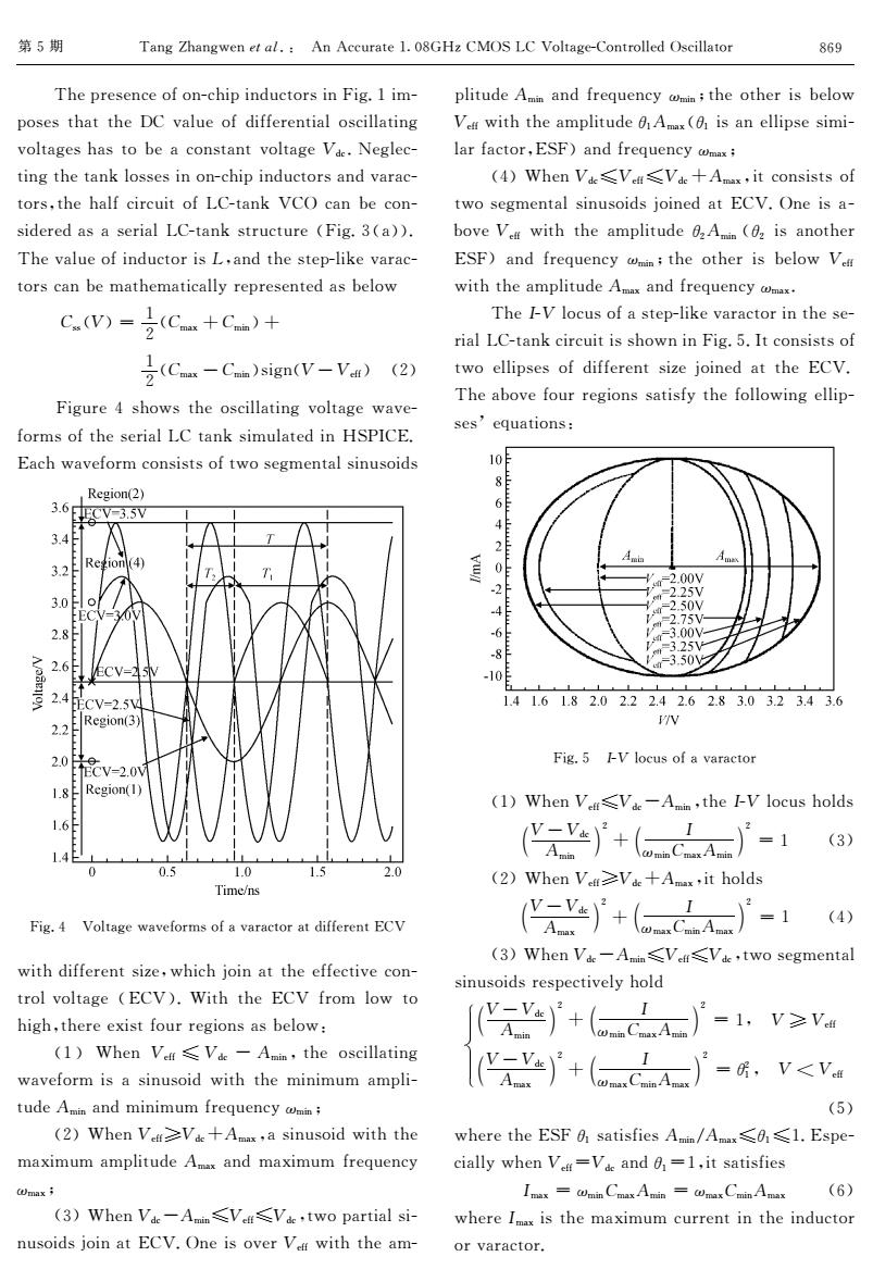
第5期 Tang Zhangwen et al.An Accurate 1.08GHz CMOS LC Voltage-Controlled Oscillator 869 The presence of on-chip inductors in Fig.1 im- plitude Amin and frequency @min the other is below poses that the DC value of differential oscillating Veu with the amplitude 6Amax(is an ellipse simi- voltages has to be a constant voltage Vde.Neglec- lar factor,ESF)and frequency cmax ting the tank losses in on-chip inductors and varac- (4)When Vde≤V.a≤Vdc十Amax,it consists of tors,the half circuit of LC-tank VCO can be con- two segmental sinusoids joined at ECV.One is a- sidered as a serial LC-tank structure (Fig.3(a)). bove Ve with the amplitude 02Amin(02 is another The value of inductor is L,and the step-like varac- ESF)and frequency wmin;the other is below Ve tors can be mathematically represented as below with the amplitude Amax and frequency @max. C.W)=2C.+C)+ The I-V locus of a step-like varactor in the se- rial LC-tank circuit is shown in Fig.5.It consists of C-C)sign(V-Va)(2) two ellipses of different size joined at the ECV. The above four regions satisfy the following ellip- Figure 4 shows the oscillating voltage wave- ses'equations: forms of the serial LC tank simulated in HSPICE. Each waveform consists of two segmental sinusoids 10F Region(2) 3.61 IECV-3.5V 6 3 0 =2.00V -2 2.25V 3.0 -4 -2.50V 2.75V -6 =3.00V 8 =3251 2.6 =3.50 ECV=25 10 2.4 ECV=2.54 1.41.61.82.02.22.42.62.83.03.23.43.6 Region(3) V 2.0 Fig.5 IV locus of a varactor ECV-2.0V Region(1) (1)When VuVa-Amin,the I-V locus holds )+ =1(3) 0.5 1.0 1.5 2.0 (2)When VeVae +Amax,it holds Time/ns Fig.4 Voltage waveforms of a varactor at different ECV '+-1 (4) (3)When Vae-Amin≤V.≤Vik,two segmental with different size,which join at the effective con- sinusoids respectively hold trol voltage (ECV).With the ECV from low to high,there exist four regions as below: y+广-v≥wm (1)When Veu <Vde-Amin,the oscillating waveform is a sinusoid with the minimum ampli- +(d广=v<v tude Amin and minimum frequency @min (5) (2)When VeVae+Amns,a sinusoid with the where the ESF 0 satisfies Amin/Amnx1.Espe- maximum amplitude Amax and maximum frequency cially when Ve=Vae and 0=1,it satisfies maxi Imax-Cmin Cmax Amin -CmaxCmin Amax (6) (3)When Vde-Amim≤Vet≤Vc,two partial si- where Imax is the maximum current in the inductor nusoids join at ECV.One is over Ve with the am- or varactor
第C期 ’*)3;=")*22=")*2VN\cR)$"8=G$1#$AA ]"2=")$#*2VN\cR)$"8*/ +=G$#$AA ]"2=")$#*22<$VN\c ’<$*+=G$A=(11$3"=)88*2"8A&2<$A=%%=]")3$%%"./ 8$8&$J(*2"=)8! @"3cC $"#%=H(8=A*G*1*H2=1 #Y$!<$)#$AA(##HgS-")"2<$$"#%=H(8<=%#8 # Z##H # S-") $ X V $ #%-")!-*TS-") $ X TY #D$ #X$!<$)#$AA&##HeS-*T""2<=%#8 # Z##H # S-*T $ X V $ #%-*T!-")S-*T $ X TY #a$ #D$!<$)##HgS-")(#$AA(##H"2]=8$3-$)2*% 8")(8="#81$8.$H2"G$%&<=%# # Z##H # S-") $ X V $ #%-")!-*TS-") $ X TY" # &#$AA # Z##H # S-*T $ X V $ #%-*T!-")S-*T $ X T&X Y" # ’# ) * + $AA #C$ ]<$1$2<$V,@&Y8*2"8A"$8S-")’S-*T(&Y(YcV8.$/ H"*%%&]<$)#$AAd##H*)#&YdY""28*2"8A"$8 $-*T T%-")!-*TS-") T%-*T!-")S-*T #W$ ]<$1$$-*T"82<$-*T"-(-H(11$)2")2<$")#(H2=1 =1G*1*H2=1c BW‘
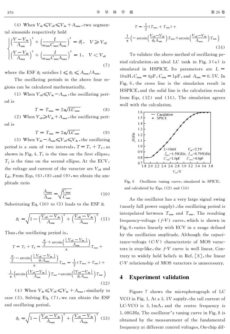
870 半导体学报 第26卷 (4)When Vae≤Vf≤Vc+Amx,two segmen- T-(T+T)十 tal sinusoids respectively hold =,V≥V (14) To validate the above method of oscillating pe- riod calculation,an ideal LC tank in Fig.3(a)is (7) where the ESF02 satisfies 1≤2≤Amax/Amim simulated in HSPICE.Its parameters are L The oscillating periods in the above four re- 10nH,Cmax =4pF,Cmin =1pF,and Amin =0.5V.In Fig.6,the cross line is the simulation result in gions can be calculated mathematically. HSPICE,and the solid line is the calculation result (1)When VeVde-Amin,the oscillating peri- from Egs.(12)and (14).The simulation agrees od is well with the calculation. T=T=2r/LCmus (8) 1.6m (2)When VeuVde+Amax,the oscillating peri- -Caculation 1.5 SPICE od is 1.4 1.3 T=Tmin =2VLCmin (9) (3)When Vae-AminVVde,the oscillating period is a sum of two intervals,T=T1+T2,as 1.0上 L=10nH 0.9F 'm-2.5V shown in Fig.4.Ti is the time on the first ellipse; 1.59GHz:-0.795GHz 0.8+ T2 is the time on the second ellipse.At the ECV, Cm=1.0pF Ca=4.0pF 0. 1.82.02.22.42.62.83.0323.43.63.8 the voltage and current of the varactor are Ve and VV I.From Eqs.(6),(8),and (9),we obtain the am- plitude ratio Fig.6 Oscillator tuning curve:simulated in SPICE. and calculated by Eqs.(12)and (14) Anin Cmin (10) As the oscillator has a very large signal swing Substituting Eq.(10)to (5)leads to the ESF (nearly full power supply),the oscillating period is interpolated between Tmax and Tmin.The resulting A-+ frequency-voltage (f-V)curve,which is shown in Fig.6,varies linearly with ECV in a range defined Thus,the oscillating period is, by the oscillation amplitude.Although the capaci- AT十 tance-voltage (CV)characteristic of MOS varac- T=T1+T= tors is step-like,the f-V curve is well linear.Con- trary to widely held beliefs in Ref.[8],the linear CV relationship of MOS varactors is unnecessary. (arcsin(Tasin() 4 Experiment validation (12) (4)When Vae<VtVde+Amax,similarly to Figure 7 shows the microphotograph of LC case (3).Solving Eq.(7),we can obtain the ESF VCO in Fig.1.At a 3.3V supply,the tail current of and oscillating period, LC-VCO is 3.1mA,and the centre frequency is 1.08GHz.The oscillator's tuning curve in Fig.8 is --)+ (13) obtained by the measurement of the fundamental frequency at different control voltages.On-chip dif-
半 导 体 学 报 第XW卷 !a"!W;9HK;>H8F @"3(1$P8<=]82<$ -"H1=.<=2=31*.< =A7N \NR")@"3cYcE2*DZD\8(..%<$2*"%H(11$)2=A 7N/\NR"8DZY-E#*)#2<$H$)21$A1$J($)H&"8 YZ[B0OUc’<$=8H"%%*2=1)82()")3H(1G$")@"3cB"8 =+2*")$#+&2<$ -$*8(1$-$)2=A2<$A()#*-$)2*% A1$J($)H&*2#"AA$1$)2H=)21=%G=%2*3$8cR)/H<".#"A/ BP[
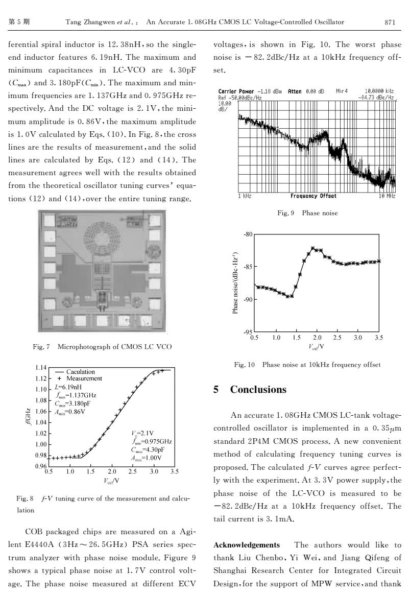
第5期 Tang Zhangwen et al.An Accurate 1.08GHz CMOS LC Voltage-Controlled Oseillator 871 ferential spiral inductor is 12.38nH,so the single- voltages,is shown in Fig.10.The worst phase end inductor features 6.19nH.The maximum and noise is -82.2dBc/Hz at a 10kHz frequency off- minimum capacitances in LC-VCO are 4.30pF set. (Cmax and 3.180pF(Cmin).The maximum and min- imum frequencies are 1.137GHz and 0.975GHz re- Carrier Power -1.18 dBa Atten 0.08 dB Mkr 4 18.0309kHz Ref -50.00dBc/Hz -84.73 dBc/Hz 18.08 spectively.And the DC voltage is 2.1V,the mini- mum amplitude is 0.86V,the maximum amplitude is 1.OV calculated by Egs.(10).In Fig.8,the cross lines are the results of measurement,and the solid lines are calculated by Eqs.(12)and (14).The measurement agrees well with the results obtained from the theoretical oscillator tuning curves'equa- tions (12)and (14),over the entire tuning range. Frequency Offset Fig.9 Phase noise -80 -85 米米 90 9 0.5 1.01.52.02.53.03.5 Fig.7 Microphotograph of CMOS LC VCO VenlV 1.14 Fig.10 Phase noise at 10kHz frequency offset Caculation 1.12 Measurement 1.10 L=6.19nH 5 Conclusions 1.08F =1.137GHz Cm=3.180pF 美1 F Am-0.86V An accurate 1.08GHz CMOS LC-tank voltage- 1.02 controlled oscillator is implemented in a 0.35um '=2.1V 1.00 m-0.975GHz standard 2P4M CMOS process.A new convenient 0.98++ C4.30pF Am=1.00V method of calculating frequency tuning curves is 0.9 0.5 1.0 1.52.0 2.53.0 3.5 proposed.The calculated f-V curves agree perfect- ValV ly with the experiment.At 3.3V power supply,the Fig.8 f-V tuning curve of the measurement and calcu- phase noise of the LC-VCO is measured to be lation -82.2dBc/Hz at a 10kHz frequency offset.The tail current is 3.1mA. COB packaged chips are measured on a Agi- lent E4440A (3Hz~26.5GHz)PSA series spec- Acknowledgements The authors would like to trum analyzer with phase noise module.Figure 9 thank Liu Chenbo,Yi Wei,and Jiang Qifeng of shows a typical phase noise at 1.7V control volt- Shanghai Research Center for Integrated Circuit age.The phase noise measured at different ECV Design,for the support of MPW service,and thank
第C期 ’*)3;@ ’<$ *(2<=18 ]=(%#%"I$2= 2<*)I 7"( N<$)+="M" !$""*)#?"*)3 :"A$)3=A ,<*)3<*"6$8$*1H< N$)2$1A=1L)2$31*2$# N"1H("2 4$8"3)"A=12<$8(..=12=AQK!8$1G"H$"*)#2<*)I BPY

872 半导体学报 第26卷 Huang Hao,Qian Dahong for chip testing. LC-VCOs'tuning curves with period calculation technique. IEEE Asia South Pacific Design Automation Conference, Shanghai.China.2005 References [5 Yue C P.Wong SS.On-chip spiral inductors with patterned ground shields for Si-based RF IC's.IEEE J Solid-State Cir- [1 Hajimiri A,Lee T H.Design issues in CMOS differential LC cuits,1998,33:743 oscillators.IEEE J Solid-State Circuits.1999.34:717 [6]http://rfic.eecs.berkeley.edu/~niknejad/asitic.html [2]Tiebout M.Low-power low-phase-noise differentially tuned [7]Hegazi E,Sjoland H,Abidi AA.A filter technique to lower quadrature VCO design in standard CMOS.IEEE J Solid- LC oscillator phase noise.IEEE J Solid-State Circuits,2001. State Circuits.2001.36:1018 36:1921 [3]Levantino S.Samori C.Bonfanti A.et al.Frequency depend- [8 Svelto F.Erratico P.Manzihi S.et al.A metal-oxide-semicon- ence on bias current in 5-GHz CMOS VCOs:impact on tuning ductor varactor.IEEE Electron Device Lett,1999.20:164 range and flicker noise upconversion.IEEE J Solid-State Cir- [9]Tang Zhangwen.LC voltage-controlled oscillators.PhD dis- cuits,2002,37:1003 sertation of Fudan University.2004 [4]Tang Zhangwen,He Jie,Jian Hongyan,et al.Prediction of 精确的1.08 GHz CMOS电感电容压控振荡器 唐长文何捷营洪彦闵吴 (复旦大学专用集成电路与系统国家重点实验室,上海200433) 摘要:在0.35um2P4M标准CMOS工艺上,设计了一个精确的1.08 GHz CMOS电感电容压控振荡器.提出了一 种有效计算压控振荡器周期的新方法,采用该方法计算的顿率-电压调谐曲线与实验结果吻合得很好.在电源电压 3.3V下,消耗电流3.1mA,压控振荡器的相位噪声在10kHz频偏处为一82.2dBc/Hz.芯片面积为0.86mm× 0.82mm. 关键词:MOS管可变电容;电感电容回路;压控振荡器;振荡调谐曲线 EEACC:1230B 中图分类号:TN752 文献标识码:A 文章编号:0253-4177(2005)05-0867-06 *上海市科学技术委员2003年度集成电路设计科技专项(批准号:037062019)和上海应用材料研究与发展基金(批准号:0425)资助项目 唐长文男,1977年出生,助理研究员,主要研究方向为低相位噪声电感电容压控振荡器和CMOS射频电视调谐器. 何捷男,1978年出生,博士研究生,主要研究方向为全集成射频频率综合器设计. 2004-10-30收到,2005-01-06定稿 ©2005中国电子学会
半 导 体 学 报 第XW卷 O(*)3O*=!:"*)4*"-"1"E!7$$’ Oc4$8"3)"88($8")NQR,#"AA$1$)2"*%7N =8H"%%*2=18cLVVV?,=%"#/,2*2$N"1H("28!Y‘‘‘!Da$PYP "X# ’"$+=(2Q c7=]/.=]$1%=]/.*#&*8"2"Hc=%*)#O!E+"#"E EcEA"%2$12$H<)"J($2=%=]$1 7N=8H"%%*2=1.<*8$)="8$cLVVV?,=%"#/,2*2$N"1H("28!X[[Y! DW$Y‘XY "B# ,G$%2=@!V11*2"H=K!Q*)U"<",!$2*%cE -$2*%/=T"#$/8$-"H=)/ #(H2=1G*1*H2=1cLVVVV%$H21=)4$G"H$7$22!Y‘‘‘!X[$YWa "‘# ’*)3;<*)3]$)c7NG=%2*3$/H=)21=%%$#=8H"%%*2=18cK<4#"8/ 8$12*2"=)=A@(#*)_)"G$18"2&!X[[a 精确的C:.EQ0[/6%1电感电容压控振荡器# 唐长文 何 捷 菅洪彦 闵 昊 ’复旦大学专用集成电路与系统国家重点实验室!上海 X[[aDD( 摘要!在[ZDC$-XKaQ 标准 NQR,工艺上!设计了一个精确的YZ[B0OUNQR,电感电容压控振荡器c提出了一 种有效计算压控振荡器周期的新方法!采用该方法计算的频率/电压调谐曲线与实验结果吻合得很好c在电源电压 DZD\ 下!消耗电流DZY-E!压 控 振 荡 器 的 相 位 噪 声 在 Y[IOU频 偏 处 为 gBXZX#5H&OUc芯 片 面 积 为 [ZBW--f [ZBX--c 关键词!QR,管可变电容)电感电容回路)压控振荡器)振荡调谐曲线 **"//$YXD[5 中图分类号!’FPCX 文献标识码!E 文章编号![XCD/aYPP"X[[C#[C/[BWP/[W #上海市科学技术委员X[[D年度集成电路设计科技专项’批准号$[DP[WX[Y‘(和上海应用材料研究与发展基金’批准号$[aXC(资助项目 唐长文 男!Y‘PP年出生!助理研究员!主要研究方向为低相位噪声电感电容压控振荡器和 NQR,射频电视调谐器c 何 捷 男!Y‘PB年出生!博士研究生!主要研究方向为全集成射频频率综合器设计c X[[a/Y[/D[收到!X[[C/[Y/[W定稿 &X[[C 中国电子学会 BPX