第26卷第8期 半导体学报 Vol.26 No.8 2005年8月 CHINESE JOURNAL OF SEMICONDUCTORS Aug.,2005 A CMOS Fully Integrated Frequency Synthesizer with Stability Compensation He Jie,Tang Zhangwen,Min Hao,and Hong Zhiliang (State Key Laboratory of ASIC System,Fudan University,Shanghai 200433,China) Abstract:A complete closed-loop third-order s-domain model is analyzed for a frequency synthesizer.Based on the model and root-locus technique,the procedure for parameters design is described,and the relationship between the process,voltage,and temperature variation of parameters and the loop stability is quantitatively analyzed.A variation margin is proposed for stability compensation.Furthermore,a simple adjustable current cell in the charge pump is proposed for additional stability compensation and a novel VCO with linear gain is adopted to limit the total varia- tion.A fully integrated frequency synthesizer from 1 to 1.05GHz with 250kHz channel resolution is implemented to verify the methods. Key words:frequency synthesizer;closed-loop third-order s-domain;loop parameters;PVT variation;stability; variation margin EEACC:1205;2570D CLC number:TN4 Document code:A Article ID:0253-4177(2005)08-1524-08 rifice performance of the phase noise and spur level 1 Introduction suppression.The better methods are to use config- urable current to compensate the change of division Monolithic frequency synthesizers based on ratio[7]and nonlinearity of VCO gainC43.However, charge pump PLL (CPLL)are prevailing in mod-these methods are of some complexity and not able ern communication systems.Loop performances,to compensate for all variation factors. such as stability,phase noise (or jitter),and switc- A CPLL based frequency synthesizer is inher- hing speed,are important design criteria and dis-ently discrete-time.Fortunately,accurate z-domain cussed in many publicationsi-6.Synthesizer de-models,state space analysis[8.9),and impulse-invar- sign is a tradeoff process to derive the parameters iant transformation io],have proven that if the loop according to specifications.Unfortunately,current,bandwidth is less than 1/20 of the reference clock, resistor,and capacitor always vary with process,s-domain model predicts the same behavior as z-do- voltage,and temperature (PVT).VCO gain is al-main models.As a result,s-domain model is also ways highly nonlinear.Variation and nonlinearity suitable for a CPLL frequency synthesizer.Tradi- tend to unstabilize the loop,especially in strict con-tionally,closed-loop s-domain model is always sim- ditions.In order to have stability,one way is to sac-plified into second.8).However,the actual Project supported by the Shanghai Science &Technology Committee,China Under System-Design-Chip(SDC)Program(No.037062019)and the Shanghai AM(Applied Material)Funds(No.0425) He Jie male,was born in 1978.PhD candidate.His research interest is in integrated RF frequency synthesizer and mixed-signal design. Tang Zhangwen male,was born in 1977,assistant professor.His research interests are in LC-VCO and CMOS RF TV tuner. Min Hao male.professor,adviser of PhD candidates.His research interests are in integrated circuit design and system integration. Received 25 November 2004,revised manuscript received 13 March 2005 ©2005 Chinese Institute of Electronics
第!#卷 第&期 !""5年&月 半 导 体 学 报 )I(+’,’.WYZ+*PWU,’A()W+1Y)/WZ, VE9>!# +E>& *NJ>$!""5 #-DE;=:F"43"#!"$%&7?R FG=,G7?JG78*A%*MM98=RA7F=D879&UN?R"2!5& I=.8= 679=$@7I8 /7?JTG7?J@=? 679=$@7I8 A8?I7E 679=$MDEH=I8 Z=:=8X=R!5+EX=6K=D!""2$D=X8J[@A PJ?H2?CKJ:J?I09RD@G>C?J9G# I=.8=$/7?JTG7?J@=?$A8?I7E$7?RIE?JTG8987?J %#=+=9N9I.+H’K+=’KI’EO#TA X #I;=98$D%1+(R(-P9K;-=I$#$+()$+- !""244$A$-(+& "K>?ACN?(*:E6M9=F=:9EB7*X7D87F8E? 67DJ8?8UNDFG=D6ED=$7*HN99L8?F=JD7F=RHD=^N=?:L Q@IP9AL>(HD=^N=?:LPEEM M=DHED67?:=,L?FG=Y?HEDFN?7F=9L$:NDD=?F$ D=V)WJ78?8V7D87F8E?7?R?E?98?=7D8FL F=?RFEN?(?EDR=DFEG7X=/G=K=FF=D6=FGERIE@=X=D$ FG= *)-PPK7UEDFN?7F=9L$7::ND7F=]0RE678? 6ER=9*/D7R80 F8E?799L$:9EIE@=X=D$FG=7:FN79
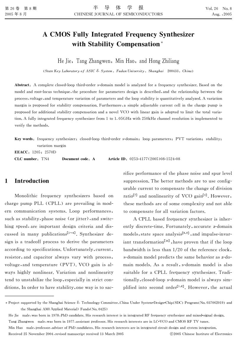
第8期 He Jie et al.A CMOS Fully Integrated Frequency Synthesizer with Stability Compensation 1525 loop is third order or even fourth order.Open-loop where K'=Kcr Kvcob s-domain model is discussed in the third orderta. NC Although an open-loop s-domain model is simple for analysis,the roughly defined phase margin is Phase Charge detector pump Low pass filter VCO indirect and not able to accurately describe the closed-loop performance and predict the effect of the parameters'PVT variation.The complete anal- ysis on the closed-loop third-order s-domain model Divider 1/N is still absent up to now. In this paper,the complete analysis on the Channel selection closed-loop third-order s-domain is performed to derive the design procedures for loop parameters. Fig.I Architecture of frequency synthesizer The effects of the parameters'PVT variation on Closed-loop transfer functions have been sim- the stability is quantitatively analyzed with the aid plified to second order and discussed in Ref.[1]. of the root locus technique.An adjustable current However,the simplified analysis will miss some cell in the charge pump is proposed to realize the implicit relationships between the parameters and damping factor control to compensate the total var- performance.The complete closed-loop third-order iation of the parameters,which is based on the vari- transfer function must be considered as following, ation analysis.A novel cross-switched VCO with NH(s) NK'(s+@z) linear gain is also adopted to reduce the total varia- H()=1+H.=+,F+K+K@, tion. NK'(s+@z) =(+20as+2)(s+mm) (3) Closed-loop third-order s-domain a- where is the nature frequency,is the damping nalysis and loop parameters factor,@ps is the closed-loop single pole. The relationship of zeros and poles between 2.1 Closed-loop third-order transfer function anal- open-loop and closed-loop is summarized as ysis 2g0n十ws=wp (4) 0+28n@ms =K' (5) In the typical CPLL frequency synthesizer wnwps =K'wz (6) with continuous-time loop filter,as shown in Fig. According to Eqs.(4)(6),the analytical equation 1,the open loop transfer function is is derived, H.(s)-KerKvea x Z(s) N (1) 2知-(42-1)w2+wp)wa+2 pWz=0(7) where Kcr is the gain of phase detector and charge Suppose @n=mwz,where m is the nature frequency pump,Z(s)is the impedance of loop filter. factor.Take it into Eq.(7),and then derive K。=g20=总×0 29m2-(4+b)m+25(b+1)=0(8) Solving Eq.(8),m can be expressed as a function 1 0.=RC:-(b+1)o of b and ,i.e.m=m(b,). From Eq.(4),the third pole @ps in the closed- Here b is the ratio between C and C2.The open loop transfer function can be expressed as loop transfer function can be rewritten as Wps (b+1-2gm)wz (9) H.(s)=K's+w: (2) which is often neglected by the second order sim- s2(s+@p) plification
第&期 I=.8=9=+>S( *)AW,UN99L(?F=JD7F=RUD=^N=?:L,L?FG=WM=?09EEM *9FGENJG7?EM=?09EEM/G=:E6M9=F=7?790 L (?FG8 /G==HH=:F*?7R;N* ?EX=9:DE + 0:9>@LW:99D?HJALW9AL@A>WL9RCJGCW GC:I>J>CGL:99DDCACR@?@A> +YE 0:9>@LW:99D?HJALW9AL@A?ACG>M@AMJ> (?FG=FLM8:79)-PP HD=^N=?:L $$FG=EM=?9EEMFD7? N)- VT)- !($5%;&V H A$ [ ;Z*] ;%;Z*M& $ *] V $ BA$ $*M V %HZ$&*] I=D=H8/G=EM=? 9EEMFD7?$ *D:G8F=:FND=EHHD=^N=?:L-$.> IE@=X=D$FG=/G=:E6M9=F=:9E /G=D=97F8E?%2&#%#&$FG=7?79LF8:79=^N7F8E? 8/7a=8F8?FE’^>%3&$7?RFG=?R=D8X= !+8! Y %2+ ! ZH&8Z!+%HZ$&V" %&& ,E9X8?J’^>%&&$8 :7?K==\MD==>8g8%H$+&S UDE6’^>%2&$FG=FG8DRME9=*M48?FG=:9E $5!5
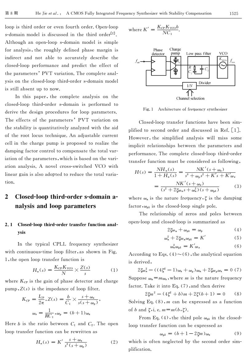
1526 半导体学报 第26卷 where n(b,is the function of b and too.Until 2.2 Loop parameters design now,the procedure to determine the loop parame- The target of loop parameters design is to a- ters is chieve the desirable loop performance.With the (P.1)Find Kvco from simulation. closed-loop analysis,it is possible to design the (P.2)Select capacitor ratio b and damping damping factor and nature frequency directly.The factor o,then calculate m,n,and k. nature frequency is always dependent on the damp- (P.3)Select loop bandwidth we according to ing factor;consequently,a damping factor could be reference clock,a good start-point:we=wre/25. set as a target at the beginning of parameter de- (P.4)Calculate zero @,@,and @s. sign,for example,=1.Capacitor ratio b should al- (P.5)Choose charge pump current Icr,and so be predefined.On the one hand,a small b makes dividing ratio N. the pole p close to the zero and results in the (P.6)Calculate R from Eq.(12),if R is too low frequency closed-loop pole @p.This can better large,increase the pump current Icp and recalculate filter high frequency noise from input and divider, R until its value is reasonable. and better attenuate clock injection spurs from the (P.7)Calculate C1,C2,if the value is too charge pump.On the other hand,b must be larger large,decrease pump current Icp,and go to P.6. than 8 for stability s.Then,might be set to 9 or 2.3 Parameters variation,stability,and margins 10 for the best possible noise performance at the beginning. Basically,loop transfer function changes with Taking on=mo:and wp=(b+1)wz into N to synthesize various frequencies.A configurable Egs.(4)and (5),gain factor K'can be expressed charge pump is used to keep the ratio N/Ker to as maintain the loop performancet7.The undeter- K'=k(b,)o (10) mined parameters variation still arises from where k(b,)is also a function of b and t,it is ex- process,temperature,and voltage.Traditionally, pressed as phase margin optimization is simple and always k(b,5)=(1-4)m2+25(b+1)m(11) used to determine the loop parameters.A prima- For K'=bIcp Kvco/2NC1,then k(b,)=bIcp X ry phase margin should be pre-defined for calcula- Kvco/2NC1,resistor R can be expressed as tion,which is usually set to about 50.However, R=2πNk(b, variation of loop parameters changes the phase bIcp Kvco - (12) margin.Phase margin optimization technique can- Loop bandwidth @e is an important parameter. not predict how much variation it can tolerate.Root As mentioned early,s-domain model is accurate in locus technique could be adopted to illustrate the the whole bandwidth only if the loop bandwidth is influence of parameters'variation.The parameters no larger than 1/20 reference frequencyt9).Because such as Icp,R,C1,C2,and Kvco will vary with PVT it is difficult to design a pretty low noise VCO in variation.What are the influences of the variation? CMOS technology,it is preferable to have a high Figure 2 is the root locus of the loop.Poles loop bandwidth.High loop bandwidth also has the migrate with the factor K'.Points B,C are the advantage of a fast switching speed.A good initial boundary to avoid under-damping behavior.To loop bandwidth is 1/25 reference frequency.From margin the loop parameter variation,for example, Eq.(2),let s=joe and H (jo)=1,with Eq. point A can be selected to identify the system,and (10),zero can be calculated as the damping factor is 1.If the gain factor K'de- 1 viates smaller than the designed value,poles will n(b,5“ (13) migrate towards point B and its conjugate pole,as
半 导 体 学 报 第!#卷 +Y+ 599DDCACR@?@A>L@>J=G /G=F7DJ=FEH9EEMM7D76=F=DS8FGFG= :9E/G= ?7FND=HD=^N=?:L8)7M7:8FEDD7F8EHW?FG=E?=G7?R$7/G8W?FG=EFG=DG7?R$H6N/G=?$H68JGFK= /7a8?J*? g 8*] 7?R*M g %Hf$&*] 8?FE ’^<>%2&7?R %5&$J78?H7:FEDNl:7?K==\MD= *B=:7NI8JG9EEMK7?R@8RFG79*JEER8?8F879 9EEMK7?R@8RFG8UDE6 ’^>%!&$9=F;g6*: 7?R17 %6*:&1g$$@8FG’^> %$"&$]=DE*]:7?K=:79:N97F=R7Y?F89 ?E@$FG=MDE:=RND=FER=F=D68?=FG=9EEMM7D76=0 F=D$&U8?RNV)WHDE6 %->!&,=9=:F:7M7:8FEDD7F8EH7?RR76M8?J H7:FED+"$FG=?:79:N97F=8$($7?RL> %->4&,=9=:F9EEMK7?R@8RFG*: 7::EDR8?JFE D=H=D=?:=:9E:a$7JEER %->2&)79:N97F=]=DE*]$*?$7?R*M4> %->5&)GEE %->#&)79:N97F=BHDE6 ’^>%$!&$8HB8 %->3&)79:N97F=A$$A!$8HFG=X79N=8#> +YT BCACR@?@A>XCAJC?J9G$>?CKJ:J?I$CGLRCA=JG> B7*:E?H8JND7K9= :G7DJ=MN6M8/G= N?R=F=D0 68?=R M7D76=F=D/D7R8F8E?799L$ MG7*MD8670 DLMG7IE@=X=D$ X7D87F8E? EH9EEM M7D76=F=D-G7ZEEF 9E:N/G=M7D76=F=DSG7F7D=FG=8?H9N=?:=-E9=-E8?F/E 67DJ8?FG=9EEMM7D76=F=DX7D87F8E?$HED=\76M9=$ ME8?FO:7?K=(HFG=J78?H7:FEDN*R=0 X87F=<<6799=DFG7?FG=R=<8J?=RX79N=$ME9=<@899 68JD7F=FE@7DR<ME8?F37?R8F<:E?;NJ7F=ME9=$7< $5!#
第8期 He Jie et al.A CMOS Fully Integrated Frequency Synthesizer with Stability Compensation 1527 well as the damping factor becoming smaller.If the here.For a small b,o=1 is acceptable approxima- gain factor K'deviates larger than the designed tion for Quantitative analysis based on third- value,poles will migrate to point C and the zero order model accurately shows the effect of parame- through the locus,as well as the damping factor ters variation on the closed-loop damping factor becoming larger at the start and then smaller after and stability.Additionally,variation margin increa- passing around point D.When poles exceed the ses with b.If the predicted variation margin cannot boundary,the loop might become under-damping. tolerate the total maximum PVT variation,then b should be increased for the large variation margin. Stability boundary- -0.707 Poles root locus 3 Circuit implementation Open-loop poles X Closed-loop poles 3.1 Phase detector Due to the slow input frequency,a phase de- 2polesaorigin tector can be implemented with the most popular D flip-flop tri-state configuration There are dead- zone elimination delay chain and differential out- puts equalization. 3.2 Charge pump with stability compensation cur- Fig.2 Root locus plot of loop rent cell and loop filter With designed damping factor to,rewrite A differential charge pump has better supply Eq.(12)to noise rejection performance and phase noise per- k(b,5o)= Kvco ICpbR2C (14) formance[iz.Figure 3 is the schematic of the 2πN charge pump.Due to differential architecture,ideal Due to the technology,temperature,and volt- matched charge pump and loop filter can eliminate age variation,the changes of Icp,Kvco,R,C,and the problems by clock feed through and charge in- Ca will disturb the closed loop poles.The actual jection. damping factor results in: However,the mismatch always exists and the k(b,0=k(b,a)=a×KveoleRC(a5) problems with the mismatch should be considered. 2πN First,level shifters are used to reduce the swings of where a is named as variation factor.Now consider switch signals to attenuate the clock feed through. the boundary condition:8=0.707,which results Half reduction of swing improves the performance amax and amin.amax is the top boundary of total pa- of reference spur suppression by 6dB.Second, rameter variation and amin is the bottom boundary. channel charge injection from switch transistors, For example,if $o=1 and b=9,then amax =1.57 e.g.PMI and NM1,can be attenuated with isola- and amin=0.65,and the loop could tolerate a total tion by saturated transistors,e.g.PM3 and NM3. 35%parameters variation at least.Variation mar- In section 2,parameters variation has been an- gin can be defined as the minimum of amax-1 and alyzed.If the total variation exceeds the boundary 1-amin.In fact,there exists an optimum variation of stability,i.e.(amin,amax),current adjustment can margin,which corresponds to an optimum damping take the loop back to the stable state.A proposed factor opt larger than o.Due to mathematical com- double-half adjustable current cell is shown in plexity,optimum damping factor is not discussed Fig.4.The current cell consists of four branches,of
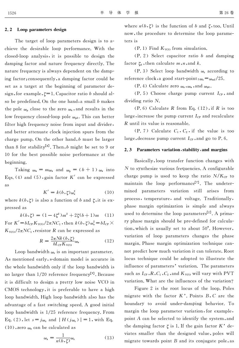
第&期 I=.8=9=+>S( *)AW,UN99L(?F=JD7F=RUD=^N=?:L,L?FG=(HFG= J78?H7:FEDN*R=X87F=SG=? ME9= U8J>! ZEEF9E:N%$!&FE L%H$+"&V NV)WT)-HB! A$ !(G %$2& 1N=FEFG=F=:G?E9EJL$F=6M=D7FND=$7?RXE9F0 7J=X7D87F8E?$FG=:G7?J=/G=7:FN79 R76M8?JH7:FEDD=+E@:E?)67\8 UED=\76M9=$8H+" g$7?RHg%$FG=?)67\ g$‘53 7?R)68?g"‘#5$7?RFG=9EEM:EN9RFE9=D7F=7FEF79 45h M7D76=F=DV7D87F8E? 67D0 J8?:7?K=R=H8?=R7(?H7:F$FG=D==\81N=FE67FG=67F8:79:E60 M9=\8FL$EMF86N6 R76M8?JH7:FED8UED7[N7?F8F7F8X=7?79L*RR8F8E?799L$X7D87F8E?67DJ8?8?:D=70 (HFG=MD=R8:F=RX7D87F8E?67DJ8?:7??EF FE9=D7F=FG=FEF7967\86N6 -V/X7D87F8E?$FG=?H T 0JAN@L@?@N?9A 1N=FEFG=/G=D=7D=R=7R0 ]E?==9868?7F8E?R=97L:G78?7?RR8HH=D=?F879ENF0 MNF TY+ 0HCA=@D?CKJ:J?IN9RD@G>C?J9GNU8JND= 4 81N=FER8HH=D=?F8797D:G8F=:FND=$8R=79 67F:G=R:G7DJ=MN6M7?R9EEMH89F=D:7?=9868?7F= FG=MDEK9=6 IE@=X=D$FG=68 U8D I79HD=RN:F8E?EH,=:E?R$ :G7??=9:G7DJ=8?;=:F8E?HDE6 J>-A$7?R+A$$:7?K=7FF=?N7F=R@8FG8J>-A47?R+A4> (?(HFG=FEF79X7D87F8E?=\:==R=>%)68?$)67\&$:NDD=?F7R;N*MDEME2>/G=:NDD=?F:=99:E?<8<F<EHHENDKD7?:G=<$EH $5!3

1528 半导体学报 第26卷 V PMO UP+ UPH+ Level UP- shifter UPH+ UPH- DNH- DNH+ UPH- (L2H) PM2 PMI DN+ DNH+ Level PM4 PM3 DN- shifter DNH- (L2H) UP+ UPL+ Level UPL- NM4 NM UP- shifter (L2L) DN+ DNL+ DNL DNL+ Level NM2 NMI DN- shifter DNL- (L2L) MO Fig.3 Differential charge pump schematic changest.The obvious improvement here is that extra variation is considered,contributed from not THDADECIEINCIINCI only N but also the charge pump current Ice,loop filter,and VCO gain Kvco. 3.3 Linear gain VCO Fig.4 Proposed current cell with double-half adjust- VCO comprises complementary cross-coupled ment negative Gm pairs and LC-tank,as shown in Fig.5. Vep and Vem are differential control nodes to in- which two are ON and two are OFF in default.If a crease the linearity of Kvco by symmetry.The tank is larger than amax,it should decrease the current Ier by disable (nDEC=0)one current branch to consists of inductor,capacitor,and cross-switched varactors.The varactors are realized by MIM ca- half the factor a.If a is smaller than amin,then in- crease Icp by enable (INC=1)two current bran- pacitors and the cross switches are realized by tran- ches to double the factor.For example,if amin sistors.Excellent linear property has been demon- 0.5,amax=1.5,△Kvco/Kvco=0.2,△Ie/I.=0.2, strated in Ref.[13].The better linear VCO gain △R/R=0.2,and△C/C1=0.l,the worst total results in smaller variation and is better for the negative variation without adjustment according to stability.Phase noise performance can also be im- Eq.(15)is 0.37,which is below amin and the loop proved with inductors L1,L2 and capacitors Cl~ tends to be under-damping.With the current doub- C3. le adjustment,the total variation factor becomes 3.4 Divider 0.74,which is acceptable.The similar half adjust- ment is for the worst positive variation.The simple A divider is implemented in ripple-like local- current cell can replace the transistor NMO and feedback architecture.The divider has a range PMO in Fig.3.There is also a complex technique from 24 to 2"+1-1.The most important benefit of that adjusts current to keep the ratio Ice/N as N the structure is to reuse the 2/3 divider cell.The
半 导 体 学 报 第!#卷 U8J>4 18HH=D=?F879:G7DJ=MN6M2 -DEME(H) 8(H)8UED=\76M9=$8H)68? g "‘5$)67\ g$‘5$,NV)W)NV)W g"‘!$,T:)T: g"‘!$ ,B)Bg"‘!$7?R ,A$)A$ g"‘$$FG= @ED%$5&8S8FGFG=:NDD=?FRENK0 9=7R;N/G=/G=4>/G=D=8/G=EKX8EN TYT 5JG@CA=CJG80% V)W:E6MD85> U:M 7?RU:? 7D=R8HH=D=?F879:E?FDE9?ER=/G=F7?a :E?/G=X7D7:FED’\:=99=?F98?=7DMDEM=DFLG7-$4.>/G=K=FF=D98?=7DV)W J78? D=-G7 TYU $JXJL@A * R8X8R=D8/G=R8X8R=DG7/G= 6E/G= $5!&
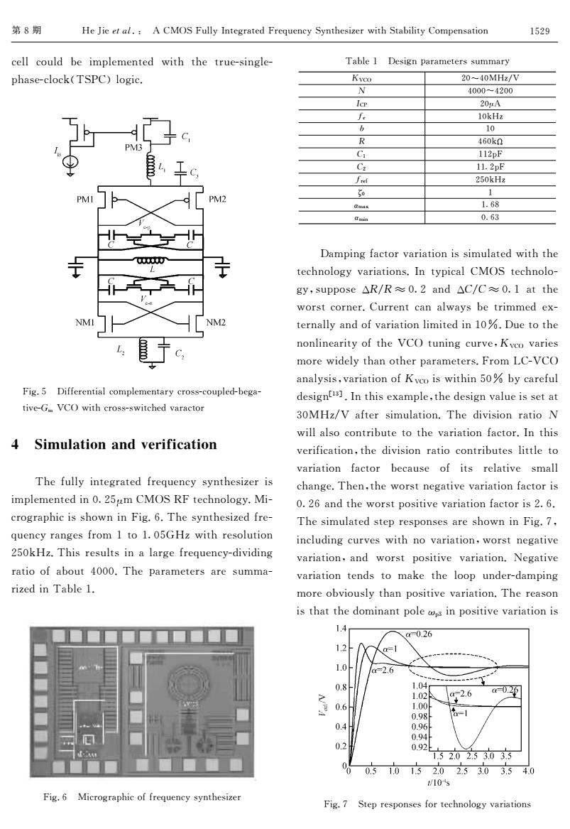
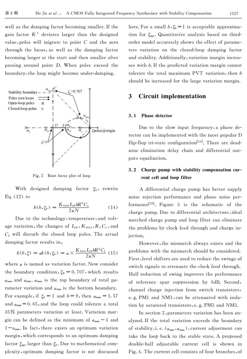
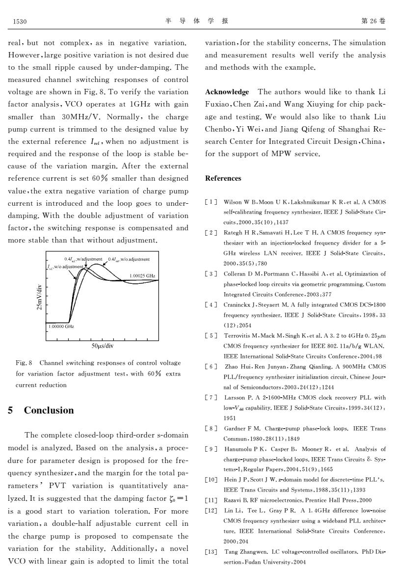
第8期 He Jie et al.A CMOS Fully Integrated Frequency Synthesizer with Stability Compensation 1529 cell could be implemented with the true-single- Table 1 Design parameters summary phase-clock(TSPC)logic. Kvco 20-40MHz/V N 4000-4200 Icp 20A fe 10kHz b 10 R 460kn PM3 C1 112pF Cz 11.2pF fre 250kHz So 1 PM PM2 (mx 1.68 Cuin 0.63 00000 Damping factor variation is simulated with the technology variations.In typical CMOS technolo- gy,suppose△R/R≈0.2and△C/C≈0.1 at the worst corner.Current can always be trimmed ex- NM NM2 ternally and of variation limited in 10%.Due to the nonlinearity of the VCO tuning curve,Kvco varies more widely than other parameters.From LC-VCO analysis,variation of Kvco is within 50%by careful Fig.5 Differential complementary cross-coupled-bega- design[.In this example,the design value is set at tive-G-VCO with cross-switched varactor 30MHz/V after simulation.The division ratio N will also contribute to the variation factor.In this 4 Simulation and verification verification,the division ratio contributes little to variation factor because of its relative small The fully integrated frequency synthesizer is change.Then,the worst negative variation factor is implemented in 0.25um CMOS RF technology.Mi- 0.26 and the worst positive variation factor is 2.6. crographic is shown in Fig.6.The synthesized fre- The simulated step responses are shown in Fig.7, quency ranges from 1 to 1.05GHz with resolution including curves with no variation,worst negative 250kHz.This results in a large frequency-dividing variation,and worst positive variation.Negative ratio of about 4000.The parameters are summa- variation tends to make the loop under-damping rized in Table 1. more obviously than positive variation.The reason is that the dominant pole @ps in positive variation is 1.4 a-0.26 1.2 a=2.6 1.04 1.02 a=2.6 0.25 0.6 1.00 0.98 a=1 0.4 0.96 0.94 0.2 0.92 1.52.02.53.03.5 00 051052025303540 t/10s Fig.6 Micrographic of frequency synthesizer Fig.7 Step responses for technology variations
第&期 I=.8=9=+>S( *)AW,UN99L(?F=JD7F=RUD=^N=?:L,L?FG= U8J>5 18HH=D=?F879:E6M9=6=?F7DL:DEA80 :DEJD7MG8:8#>/G=/G8/G=M7D76=F=D U8J># A8:DEJD7MG8:EHHD=^N=?:L(?FLM8:79)AW,F=:G?E9E0 JL$)NDD=?F:7?79@7L1N=FEFG= ?E?98?=7D8FLEHFG=V)WFN?8?J:NDX=$NV)W X7D8=UDE6P)0V)W 7?79L(?FG8/G=R8X8(?FG8/G=?$FG=@ED /G=3$ 8?:9NR8?J:NDX=+=J7F8X= X7D87F8E?F=?R/G=D=73 ,F=MD=<ME?<=<HEDF=:G?E9EJLX7D87F8E?< $5!%
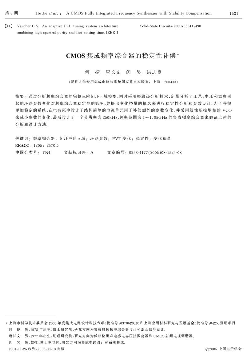
1530 半导体学报 第26卷 real,but not complex,as in negative variation. variation,for the stability concerns.The simulation However,large positive variation is not desired due and measurement results well verify the analysis to the small ripple caused by under-damping.The and methods with the example. measured channel switching responses of control voltage are shown in Fig.8.To verify the variation Acknowledge The authors would like to thank Li factor analysis,VCO operates at 1GHz with gain Fuxiao,Chen Zai,and Wang Xiuying for chip pack- smaller than 30MHz/V.Normally,the charge age and testing.We would also like to thank Liu pump current is trimmed to the designed value by Chenbo,Yi Wei,and Jiang Qifeng of Shanghai Re- the external reference Ief,when no adjustment is search Center for Integrated Circuit Design,China, required and the response of the loop is stable be- for the support of MPW service. cause of the variation margin.After the external reference current is set 60%smaller than designed References value,the extra negative variation of charge pump current is introduced and the loop goes to under- [1]Wilson W B.Moon U K.Lakshmikumar K R.et al.A CMOS damping.With the double adjustment of variation self-calibrating frequency synthesizer.IEEE J Solid-State Cir- cuits,2000,35(10):1437 factor,the switching response is compensated and [2 Rategh H R.Samavati H.Lee T H.A CMOS frequency syn- more stable than that without adjustment. thesizer with an injection-locked frequency divider for a 5- GHz wireless LAN receiver.IEEE J Solid-State Circuits. 0.4/.w/adjustment 0.4/w/o.adjustment 2000.35(5):780 1.00025GHz 3 Colleran D M.Portmann C.Hassibi A.et al.Optimization of phase-locked loop circuits via geometric programming.Custom Integrated Circuits Conference.2003:377 [4]Craninckx J.Steyaert M.A fully integrated CMOS DCS-1800 frequency synthesizer.IEEE J Solid-State Circuits,1998.33 1.00000 GHz (12):2054 [5]Terrovitis M.Mack M.Singh K.et al.A 3.2 to 4GHz 0.25gm 50μs/div CMOS frequency synthesizer for IEEE 802.11a/b/g WLAN. IEEE International Solid-State Circuits Conference.2004:98 Fig.8 Channel switching responses of control voltage [6]Zhao Hui.Ren Junyan.Zhang Qianling.A 900MHz CMOS for variation factor adjustment test,with 60%extra PLL/frequency synthesizer initialization circuit.Chinese Jour- current reduction nal of Semiconductors.2003.24(12):1244 [7]Larsson P.A 2-1600-MHz CMOS clock recovery PLL with 5 Conclusion low-Va capability.IEEE J Solid-State Circuits.1999.34(12): 1951 [8]Gardner F M.Charge-pump phase-lock loops.IEEE Trans The complete closed-loop third-order s-domain Commun,1980,28(11):1849 model is analyzed.Based on the analysis,a proce- [9]Hanumolu P K.Casper B.Mooney R.et al.Analysis of dure for parameter design is proposed for the fre- charge-pump phase-locked loops.IEEE Trans Circuits Sys- quency synthesizer,and the margin for the total pa- tems-I:Regular Papers.2004.51(9):1665 [10]Hein J P,Scott J W.z-domain model for discrete-time PLL's. rameters'PVT variation is quantitatively ana- IEEE Trans Circuits and Systems,1988,35(11):1393 lyzed.It is suggested that the damping factor o=1 [11]Razavi B.RF microelectronics.Prentice Hall Press.2000 is a good start to variation toleration.For more [12]Lin Li.Tee L.Gray P R.A 1.4GHz difference low-noise variation,a double-half adjustable current cell in CMOS frequency synthesizer using a wideband PLL architec- ture.IEEE International Solid-State Circuits Conference, the charge pump is proposed to compensate the 2000:204 variation for the stability.Additionally,a novel [13]Tang Zhangwen.LC voltage-controlled oscillators.PhD Dis- VCO with linear gain is adopted to limit the total sertion.Fudan University.2004
半 导 体 学 报 第!#卷 D=79$KNF?EF:E6M9=\$7 IE@=X=D$97DJ=ME/G= 6=7&>/EX=D8HLFG=X7D87F8E? H7:FED7?79L+ED6799L$FG= :G7DJ= MN6M:NDD=?F8*HF=DFG==\F=D?79 D=H=D=?:=:NDD=?F8S8FGFG=RENK9=7R;N U8J>& )G7??=9J9G /G=:E6M9=F=:9EB7(F8UED 6ED= X7D87F8E?$7RENK9=0G79H7R;N*RR8F8E?799L$7 ?EX=9 V)W@8FG98?=7DJ78?8/G= "NVG9P:@L=@ /G=7NFGEDS=@EN9R79 4@M@A@GN@> -$. S89*)AW, (’’’.,E98R0,F7F=)8D0 :N8F*)AW,HD=^N=?:L(’’’ . ,E98R0,F7F= )8D:N8FWMF868]7F8E?EH MG7)N*HN99L8?F=JD7F=R)AW,1),0$&"" HD=^N=?:L(’’’.,E98R0,F7F=)8D:N8F*4‘!FE2CI]"‘!5$6 )AW,HD=^N=?:L (’’’(?F=D?7F8E?79,E98R0,F7F=)8D:N8F*%""AI])AW, -PP)HD=^N=?:L)G8?=*!0$#""0AI])AW,:9E:aD=:EX=DL-PP @8FG 9E@0URR:7M7K898FL>(’’’.,E98R0,F7F=)8D:N8F)G7DJ=0MN6MMG7(’’’ /D7?*?79L(’’’/D7?]0RE678?6ER=9HEDR8 (’’’/D7?ZU68:DE=9=:FDE?8:<>-D=?F8:=I799-D=* $‘2CI]R8HH=D=?:=9E@0?E8(’’’ (?F=D?7F8E?79 ,E98R0,F7F= )8D:N8FP)XE9F7J=0:E?FDE99=RE-G118<0 <=DF8E?$UNR7?Y?8X=D<8FL$!""2 $54
第8期 He Jie et al.A CMOS Fully Integrated Frequency Synthesizer with Stability Compensation 1531 [14]Vaucher C S.An adaptive PLL tuning system architecture Solid-State Circuits.2000.35(4):490 combining high spectral purity and fast setting time.IEEE J CMOS集成频率综合器的稳定性补偿 何捷唐长文闵昊洪志良 (复旦大学专用集成电路与系统国家重点实验室,上海200433) 摘要:通过分析频率综合器的完整三阶闭环$域模型,同时采用根轨迹分析技术,定量分析了工艺、电压和温度引 起的环路参数变化对频率综合器稳定性的影响,并提出变化裕量的概念来进行稳定性分析和参数设计,为了获得 更加稳定的系统,在电荷泵中设计了结构简单的电流单元用于补偿额外的参数变化,并采用线性压控增益的VCO 来减小参数的变化.最后设计了一个分辨率为250kHz,频率范围为1~1.05GHz的集成频率综合器来验证上述的 分析和设计方法 关键词:频率综合器;闭环三阶s域:环路参数;PVT变化:稳定性;变化裕量 EEACC:1205:2570D 中图分类号:TN4 文献标识码:A文章编号:0253-4177(2005)08-1524-08 上海市科学技术委员会2003年度集成电路设计科技专项(批准号:037062019)和上海应用材料研究与发展基金(批准号:0425)资助项目 何捷男,1978年出生,博士研究生,研究方向为集成射频频率综合器设计和混合信号设计 唐长文男,19?7年出生,助理研究员,研究方向为低相位噪声电感电容压控振荡器和CMOS射频电视调谐器. 闵吴男,教授,博士生导师,研究方向为集成电路设计和系统集成 2004-11-25收到,2005-03-13定稿 ⊙2005中国电子学会
第&期 I=.8=9=+>S( *)AW,UN99L(?F=JD7F=RUD=^N=?:L,L?FG=*?7R7MF8X=-PPFN?8?J(’’’. ,E98R0,F7F=)8D:N8F为了获得 更加稳定的系统$在电荷泵中设计了结构简单的电流单元用于补偿额外的参数变化$并采用线性压控增益的 V)W 来减小参数的变化>最后设计了一个分辨率为!5"aI]$频率范围为$#$‘"5CI]的集成频率综合器来验证上述的 分析和设计方法> 关键词#频率综合器,闭环三阶 唐长文 男$$%33年出生$助理研究员$研究方向为低相位噪声电感电容压控振荡器和 )AW,射频电视调谐器> 闵 昊 男$教授$博士生导师$研究方向为集成电路设计和系统集成> !""20$$0!5收到$!""50"40$4定稿 "!""5 中国电子学会 $54$